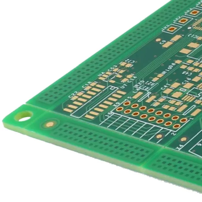
Developing an electronic product requires more than designing a circuit that works in theory. The electrical connections must eventually be translated into a physical structure that can be manufactured, assembled, and tested. This process begins with a circuit diagram, also known as a schematic, which uses standard symbols to represent electronic components such as resistors, capacitors, diodes, transistors, and integrated circuits. Although a schematic explains how the circuit operates electrically, it does not define the actual positions, dimensions, or copper connections required for manufacturing.
To turn this electrical concept into a functional printed circuit board, designers need to understand how to convert a circuit diagram into a PCB layout. PCB design software bridges the gap between logical circuit connections and the physical board by providing tools for component placement, trace routing, layer configuration, and design verification.
Popular PCB design platforms include Altium Designer, KiCad, Proteus, EAGLE, and EasyEDA. These tools help engineers develop board layouts, identify design problems, and prepare manufacturing data before production begins. A well-planned conversion process can improve electrical performance, simplify assembly, reduce manufacturing risks, and support reliable product development.

Steps Involved in Preparing PCB Layout
Converting a circuit schematic into a PCB layout involves several connected stages. Each stage contributes to the accuracy, manufacturability, and performance of the finished board. Incorrect footprints, unsuitable component placement, or incomplete routing can lead to assembly difficulties and electrical failures. Following a structured workflow helps designers identify potential problems before sending the design for fabrication.
Circuit Schematic Design – Begin by creating or reviewing the circuit schematic in suitable PCB design software. The schematic should accurately represent every required component, electrical connection, power source, ground connection, and signal path. Component reference designators, pin assignments, and polarity information must also be correct. Electrical rule checks can help identify issues such as unconnected pins, conflicting power connections, and unintended connection errors before the design moves to the layout stage. A complete schematic provides the electrical foundation for converting the circuit diagram into a PCB layout.
Component Footprint Assignment – Each schematic symbol must be associated with a suitable physical footprint. A footprint defines the pad arrangement, pad dimensions, spacing, and other package-related details used on the actual PCB. Select footprints that match the intended component's datasheet and commercially available package. For example, two components with similar electrical functions may have different pin spacing or package dimensions. An incorrect footprint can prevent proper soldering or make the component impossible to mount. Verifying package specifications early helps avoid costly redesigns and supports accurate component sourcing.
PCB Outline Creation – Define the board's external dimensions according to the enclosure, installation environment, and product requirements. The outline should include any necessary mounting holes, cutouts, slots, edge clearances, and connector openings. Consider mechanical constraints such as screw positions, enclosure walls, heat sinks, and cable access before finalizing the board shape. For projects involving large production volumes, panelization may also be planned to arrange multiple boards within a manufacturing panel. A clear and accurate PCB outline helps ensure that the finished board fits the intended product.

Components Placement – Arrange the components within the board outline while considering electrical performance, mechanical restrictions, assembly efficiency, and maintenance requirements. Related components should generally be positioned close enough to support their intended circuit functions. For example, decoupling capacitors are commonly placed near the power pins of integrated circuits, while connectors should align with the enclosure and external interfaces. Sensitive analog circuits, switching power components, and high-speed digital signals may require careful separation to reduce interference. Check component orientation, polarity, pin accessibility, thermal requirements, and clearance before proceeding to routing.
Traces Routing – Once the component arrangement is established, connect the pads according to the schematic's electrical netlist using copper traces. Routing decisions influence signal integrity, power delivery, electromagnetic compatibility, and manufacturing reliability. Trace width should be selected based on current requirements, copper thickness, temperature rise, and applicable design constraints. High-speed signals may require controlled impedance, appropriate reference planes, and careful attention to return-current paths. Avoid unnecessary detours and sharp routing geometry where practical, and maintain the required spacing between different electrical nets. PCB routing should balance electrical performance with efficient use of board space.
Addition of Vias and Planes – When a design uses multiple copper layers, vias provide electrical connections between appropriate layers. Through-hole vias pass through the board, while blind and buried vias connect selected layers without extending through the entire board. The appropriate structure depends on the layer stack-up, routing density, electrical requirements, and manufacturing budget. Copper planes are also commonly used for ground and power distribution, providing low-impedance paths and, when properly designed, useful reference planes for signal routing. A carefully planned multilayer PCB layout can accommodate complex circuits within limited space, but layer configuration and via selection should be coordinated with the manufacturer's capabilities.
Design Rule Check (DRC) – Before generating manufacturing files, run the PCB design software's Design Rule Check to identify potential layout violations. Typical checks cover trace spacing, minimum conductor width, pad-to-trace clearance, copper-to-board-edge distance, drill constraints, and unconnected nets. Additional checks may be required for high-speed interfaces, controlled-impedance routing, thermal design, and assembly clearances. Review each warning or error instead of assuming that the software has automatically confirmed the design is ready for production. Electrical Rule Check (ERC) on the schematic and DRC on the PCB serve different purposes, so both should be completed as appropriate. A final review against the manufacturer's fabrication capabilities helps reduce production delays and avoid preventable defects.
Gerber File Generation – After completing layout verification, export the manufacturing data required by the PCB fabricator. Gerber files commonly describe individual copper layers, solder mask layers, and silkscreen layers, while NC drill files provide hole-location and drilling information. Depending on the manufacturer and design workflow, additional information may be required for the board outline, stack-up, surface finish, controlled impedance, or other fabrication specifications. Assembly usually requires separate documentation, such as a bill of materials (BOM), pick-and-place data, and assembly drawings. Gerber files do not automatically contain every component or assembly instruction. Before submitting the package, confirm that all required files are present, correctly named, and consistent with the final PCB revision.
Some Useful Points to Consider
PCB layout preparation determines how effectively an electronic circuit can be manufactured and integrated into its intended product. A design that appears correct on the screen may still encounter problems if component dimensions, electrical constraints, thermal conditions, or manufacturing tolerances are overlooked. Applying good layout practices throughout the design process can reduce revisions and improve the reliability of the finished board.
Use clear component reference designators. Assign readable identifiers such as R1, C1, D1, and U1. Ensure that silkscreen labels do not overlap pads, cover important markings, or become difficult to read after assembly.
Optimize trace routing. Keep connections reasonably direct while respecting electrical and manufacturing requirements. Avoid unnecessary bends and long routing paths, and pay particular attention to sensitive signals, high-current connections, and high-speed interfaces.
Allow sufficient component spacing. Prevent footprint overlap and maintain suitable clearances for soldering, inspection, thermal dissipation, and mechanical installation. Components that generate significant heat may need additional copper area or separation from temperature-sensitive parts.
Verify electrical connectivity. Check that all intended nets are connected and that no unwanted shorts exist. Review both the schematic and PCB netlist, and confirm the ground and power distribution strategy before fabrication.
Confirm component orientation and polarity. Check pin numbering, diode direction, capacitor polarity, connector orientation, and integrated-circuit placement against the schematic and datasheets. Clear polarity markings can also reduce assembly mistakes.
Validate input and output interfaces. Ensure that connectors, power inputs, signal ports, and communication interfaces match the system requirements. Verify voltage levels, current capacity, pin assignments, and relevant protection circuitry.
Choose components with verified footprints. Use manufacturer datasheets and reliable library information rather than relying solely on generic package names. Confirm that selected components are available and that their footprints match the actual parts intended for assembly.
Consider thermal and manufacturing constraints. Check copper thickness, minimum trace width and spacing, drill sizes, board thickness, and surface finish against the fabricator's capabilities. Components that dissipate significant power may require thermal calculations or additional cooling provisions.
Review the final manufacturing package. Open the exported layers in a Gerber viewer and inspect the board outline, copper patterns, solder mask, silkscreen, and drill data. This independent review can reveal export or configuration errors that were not obvious in the design editor.
Summary
Understanding how to convert a circuit diagram into a PCB layout is essential for transforming an electronic concept into a manufacturable product. The process involves more than transferring connections onto a board: designers must verify the schematic, assign accurate footprints, define mechanical dimensions, place components, route copper traces, configure layers, and validate the complete design before generating production files.
Each stage affects the next, so careful planning and repeated verification are important. By following a consistent PCB design workflow and checking electrical, mechanical, and manufacturing requirements, engineers can reduce avoidable errors and improve the likelihood of a successful first production run.