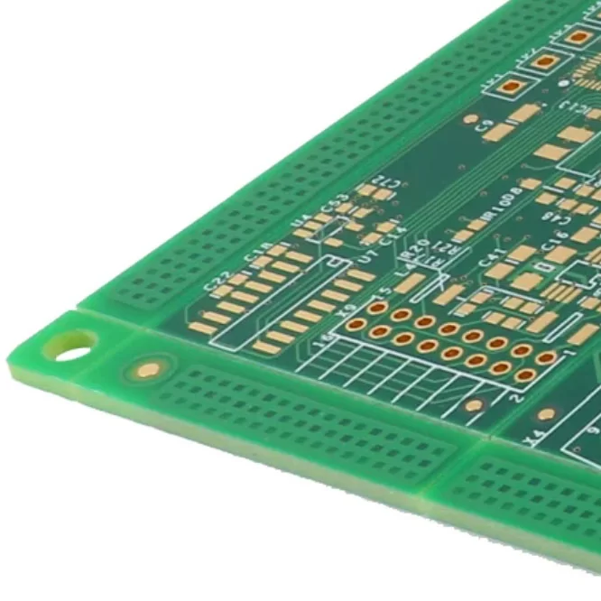
Soldering is a fundamental skill in electronics, supporting everything from assembling simple hobby circuits to manufacturing complex electronic systems. A printed circuit board (PCB) relies on properly formed solder joints to connect components to conductive pads, maintain electrical continuity, and withstand the mechanical and thermal demands of everyday operation.
Achieving consistent soldering results involves more than applying heat and melting solder. Operators must select suitable tools, control the temperature, prepare the surfaces, position components accurately, and inspect completed joints. Whether you are building a prototype, repairing an electronic device, or managing a production process, understanding how to solder on PCB can help improve assembly quality and reduce avoidable defects. This guide covers the essential tools, soldering methods, inspection procedures, safety measures, and repair practices used in PCB assembly.

What is PCB Soldering?
PCB soldering is the process of joining electronic components to conductive pads on a printed circuit board using a suitable solder alloy. When heated correctly, the solder melts and wets the metal surfaces, forming an electrical connection and helping secure the component in position after cooling.
This process is widely used in electronics manufacturing, prototype development, product maintenance, and circuit board repair. Depending on the board design and component package, soldering may be performed manually or through automated production equipment. Reliable results depend on suitable materials, controlled heating, clean surfaces, and correct component placement.
How PCB Soldering Works
During soldering, heat is applied to the component terminal and the corresponding PCB pad so that the solder can melt and wet both surfaces. Once the heat source is removed, the solder cools and solidifies, creating a conductive joint.
A successful connection requires adequate wetting, appropriate solder volume, and a suitable thermal profile. Insufficient heat may result in incomplete wetting, while excessive heat can damage components, copper pads, or the PCB substrate. Understanding this balance is central to achieving dependable solder joints.
Leaded vs. Lead-Free Solder
Leaded solder alloys, such as tin-lead formulations, generally melt at lower temperatures and are often easier to handle during manual rework. However, their use is restricted in many applications because of environmental regulations, including the European Union's RoHS requirements.
Lead-free alloys, commonly based on tin with other metals such as silver or copper, typically require higher processing temperatures. They are widely used in modern electronics manufacturing and can deliver reliable connections when the materials, equipment, and process parameters are properly controlled. The correct alloy should be selected according to product requirements, applicable regulations, and compatibility with existing joints.
Where PCB Soldering is Used
PCB soldering is essential across numerous industries, including consumer electronics, automotive systems, telecommunications, industrial automation, medical equipment, aerospace, and renewable energy technologies. It connects components in devices ranging from household appliances and communication modules to industrial controllers and specialized electronic instruments.
Different applications impose different requirements for thermal stability, vibration resistance, electrical performance, and long-term reliability. For this reason, the soldering process must be matched to the intended operating environment and the specifications of the electronic assembly.
Why Proper PCB Soldering is Important
Solder joint quality directly affects the electrical performance, mechanical stability, and service life of a PCB assembly. Even when components and board materials meet their specifications, poor soldering can introduce faults that lead to intermittent operation, production delays, or premature product failure.
Creates Strong Mechanical Connections. Solder joints help hold component terminals in place while maintaining contact with the PCB pads. Correctly formed joints can withstand normal handling, vibration, and thermal cycling within the limits of the design. Inadequate bonding, however, may allow cracks or intermittent connections to develop during service.
Reduces Product Failures. Incorrect solder volume, incomplete wetting, solder bridges, and cracked joints can all affect circuit operation. Following a controlled PCB soldering process helps reduce these defects and lowers the likelihood of troubleshooting, rework, and field repairs.
Improves Manufacturing Quality. Standardized soldering procedures help manufacturers achieve repeatable results across production batches. Consistent temperature control, material selection, equipment maintenance, and inspection improve process stability, increase production yield, and support compliance with applicable workmanship requirements.
Provides Reliable Electrical Connections. A properly formed solder joint creates a conductive path between the component terminal and the PCB pad. Low-resistance connections help maintain the intended flow of power and signals, while reducing the risk of voltage drops, unstable operation, and intermittent electrical faults.
Tools Required for PCB Soldering
Before learning how to solder on PCB, prepare the equipment required for component handling, heat application, solder removal, and inspection. Suitable tools make it easier to work accurately while reducing the risk of damaging delicate components or copper pads.
Soldering Iron
A temperature-controlled soldering iron is commonly used for manual assembly and repair. It heats the joint to the required temperature, allowing solder to flow between the component terminal and PCB pad. Different tip shapes and sizes are available to suit through-hole connections, small surface-mount parts, and larger thermal pads.
Wire for Soldering
Solder wire provides the alloy needed to form the joint. Flux-cored solder is commonly used for manual work because the flux helps improve wetting during heating. The alloy composition and wire diameter should be selected according to the assembly requirements, applicable environmental standards, and component specifications.
Flux
Flux helps remove or disrupt surface oxides and improves solder wetting. It is particularly useful when working with oxidized pads, fine-pitch components, or older assemblies. Flux is available in different formulations, including liquid, paste, and gel types. Choose a product compatible with the soldering process and clean any residues when required.
Solder Wick and Desoldering Pump
Solder wick absorbs molten solder through capillary action, making it useful for removing excess solder and clearing bridges between nearby pads. A desoldering pump uses suction to extract molten solder, particularly from through-hole joints. These tools are valuable during component replacement and corrective rework.
Tweezers and PCB Holder
Precision tweezers help position small components and hold them steady during soldering. A PCB holder or fixture secures the board and provides better access to the working area. Stable positioning is especially important when handling fine-pitch surface-mount devices or performing detailed repair work.
Magnification and Lighting
Good illumination and magnification make it easier to identify solder bridges, incomplete joints, misaligned components, and damaged pads. Magnifying lamps and digital microscopes are useful for inspecting small packages and densely populated boards, where defects may be difficult to detect with the naked eye.
Recommended Soldering Temperatures
Typical soldering iron settings for manual work may fall within approximately 315°C to 350°C for common leaded solder alloys and 350°C to 380°C for many lead-free applications. These are starting ranges rather than universal settings. The appropriate temperature depends on the solder alloy, tip geometry, joint size, PCB copper area, and component heat sensitivity. Use the lowest practical setting that allows the joint to be completed efficiently, and follow the material and component manufacturers' recommendations whenever available.
Types of PCB Soldering Techniques
The most suitable soldering method depends on component technology, production volume, board layout, and quality requirements. Manual techniques provide flexibility for prototypes and repairs, while automated processes are designed to deliver repeatable results across larger production runs.
1. Hand Soldering
Hand soldering uses a soldering iron to join individual component terminals to PCB pads. The operator controls the tool, solder feed, and heating time, making this method suitable for prototypes, small production batches, component replacement, and localized rework.
Its main advantages are low equipment requirements and the ability to access specific joints. However, quality depends heavily on operator skill, making consistent technique and inspection important when working on multiple boards.
2. Reflow Soldering
Reflow soldering is widely used for surface-mount technology (SMT) assembly. Solder paste is deposited onto the appropriate pads, components are placed in position, and the board passes through a reflow oven according to a controlled thermal profile.
As the temperature rises, the solder particles melt and form connections between component terminals and PCB pads. The board then cools under controlled conditions. Reflow soldering supports high-density assemblies and automated production, provided that solder paste deposition, placement accuracy, and thermal parameters are properly managed.
3. Wave Soldering
Wave soldering is commonly used for through-hole components and selected mixed-technology assemblies. The PCB moves across a controlled wave of molten solder, which contacts exposed solderable surfaces and forms multiple joints during a single pass.
This technique can process many connections efficiently and is particularly useful for high-volume manufacturing. Its suitability depends on component layout, board clearance, thermal requirements, and the presence of surface-mount components that may be affected by the process.
4. Selective Soldering
Selective soldering applies molten solder to specific joints rather than exposing the entire board to a solder wave. A programmed system targets designated through-hole connections while controlling flux application, preheating, and solder contact.
It is especially useful for mixed-technology PCBs containing both SMT and through-hole components, where only certain joints require wave-type soldering. Selective soldering can reduce unnecessary thermal exposure and provide precise control, although equipment setup and programming require additional investment.
5. Choosing the Right Soldering Technique
Selecting a soldering method requires consideration of component types, circuit density, production quantity, thermal sensitivity, equipment availability, and total manufacturing cost. Hand soldering is practical for prototypes and isolated repairs because it requires relatively little equipment. Reflow soldering is generally preferred for SMT production, while wave and selective soldering can be suitable for through-hole connections in larger manufacturing runs.
For assemblies that combine different component technologies, manufacturers may use more than one method. The objective is to choose a process that achieves reliable joints while maintaining production efficiency and protecting heat-sensitive components.
PCB Soldering Techniques Comparison
Soldering Method | Best Application | Main Advantages | Disadvantages |
Hand Soldering | Prototypes, repairs, and small batches | Flexible, relatively low equipment cost, suitable for targeted work | Slower and more dependent on operator skill |
Reflow Soldering | SMT assembly | Repeatable results, supports fine-pitch parts, suitable for automation | Requires solder paste control, placement equipment, and a reflow oven |
Wave Soldering | High-volume through-hole assembly | Processes many joints efficiently | Less suitable for some dense SMT layouts and heat-sensitive components |
Selective Soldering | Mixed-technology assemblies | Targets specific joints and limits unnecessary solder exposure | Higher equipment and programming requirements |
How to Inspect Solder Joints
Inspecting solder joints is a critical step in verifying PCB assembly quality. A circuit may appear to function initially while still containing weak joints or hidden defects that develop into failures after repeated thermal or mechanical stress. Appropriate inspection helps identify problems before the board is released for use.
Visual Inspection
Visual inspection is a basic and widely used method for checking solder joint appearance and component placement. Depending on the component package and soldering process, acceptable joints should show suitable wetting, appropriate solder coverage, and no unintended bridges or visible cracks.
Check for insufficient solder, excess solder, lifted pads, component misalignment, and signs of overheating. Because appearance alone cannot reveal every defect, visual inspection should be combined with electrical testing or specialized inspection when necessary.
Automated Optical Inspection (AOI)
Automated Optical Inspection uses cameras and image-processing software to examine assembled PCBs. AOI systems can identify visible defects such as missing components, incorrect orientation, placement errors, solder bridges, and certain solder joint irregularities.
This method is widely used in production because it provides repeatable inspection at higher speeds than manual examination. However, AOI cannot directly inspect solder joints hidden beneath many component packages, so other methods may be needed for those areas.
X-Ray Inspection
X-ray inspection is used to evaluate solder connections that cannot be seen from the surface. It is particularly valuable for packages such as Ball Grid Arrays (BGAs) and other components with concealed terminals.
Depending on the inspection system and joint geometry, X-ray analysis can reveal defects such as solder bridging, voids, and irregular solder structures. It complements visual inspection and AOI by providing information about hidden connections that could otherwise remain undetected.
Good vs. Bad Solder Joints
A good solder joint generally exhibits proper wetting between the component terminal and the PCB pad, with sufficient solder to establish the intended connection. Its exact appearance varies according to the component type, solder alloy, and assembly process.
Potential defects include cracks, incomplete wetting, insufficient solder, unintended bridges, and excessive solder buildup. A dull or irregular appearance may indicate a problem in some situations, but visual appearance alone is not conclusive. Electrical testing and process-specific acceptance criteria should be used to confirm suspected defects.
IPC Quality Standards
IPC-A-610 provides acceptance criteria for electronic assemblies, while IPC J-STD-001 specifies requirements for soldered electrical and electronic assemblies. These standards are widely referenced in electronics manufacturing to establish workmanship expectations and inspection requirements.
The applicable class, product requirements, and contract specifications determine which acceptance criteria should be followed. Using the appropriate standards helps align soldering practices, inspection procedures, and quality expectations across production teams.

PCB Soldering Tips & Best Practices
Consistent soldering results depend on proper preparation, controlled heating, suitable materials, and careful inspection. Applying the following practices can help improve joint quality and reduce avoidable rework.
Keep the Soldering Iron Tip Clean. Oxidized or contaminated tips transfer heat less efficiently and may prevent solder from flowing smoothly. Clean the tip regularly using a suitable brass cleaner or approved sponge, and maintain appropriate tip condition throughout the work.
Heat the Pad and Component Together. When learning how to solder PCB connections, place the iron tip so that it transfers heat to both the PCB pad and the component terminal. Feed solder into the heated joint rather than relying on melting solder directly against the iron tip. This helps the solder wet both surfaces and form a more reliable connection.
Use the Correct Amount of Solder. The solder volume should be sufficient to establish a sound joint without covering neighboring pads or obscuring important features. Excess solder can create bridges, while insufficient solder may result in weak or incomplete connections. Use the pad and component geometry as a guide.
Maintain Proper Soldering Temperature. Select a temperature appropriate for the alloy, joint size, and thermal characteristics of the board. Too little heat can prevent proper wetting, while excessive heat or prolonged contact may damage components and lift pads. Consistent process settings help improve repeatability.
Keep the PCB Surface Clean. Oil, dust, oxidation, and other contaminants can interfere with solder wetting. Use suitable cleaning methods before soldering when necessary, and remove flux residues according to the flux manufacturer's recommendations and the product's cleanliness requirements.
PCB Soldering Safety Guidelines
PCB soldering involves hot tools, chemical fumes, and potentially sensitive electrical assemblies. A safe workstation helps protect the operator, preserve components, and reduce the likelihood of accidental damage.
Work in a Well-Ventilated Area
Flux fumes generated during soldering may irritate the eyes and respiratory system. Work in a properly ventilated area, preferably with local fume extraction positioned near the soldering point. Avoid breathing directly over the joint, and follow the safety instructions supplied with the solder and flux materials.
Personal Protective Equipment (PPE)
Safety glasses help protect the eyes from accidental solder splashes and clipped leads. Wear clothing suitable for the task and avoid loose items that could contact hot equipment. Gloves are not always appropriate for precision soldering, so use protective equipment based on the task's risk assessment and maintain careful handling practices.
Prevent Electrostatic Discharge
Electrostatic discharge can damage sensitive integrated circuits and other electronic components, even when the damage is not immediately visible. Use an appropriate ESD-protected workstation, grounded tools, and a wrist strap connected according to established ESD procedures. Follow the required precautions when handling exposed semiconductor devices.
Handle Hot Equipment Carefully
Soldering iron tips can reach temperatures well above 300°C and may cause serious burns. Place the iron in a stable stand whenever it is not in use, keep hot tools away from cables and combustible materials, and allow equipment to cool before storage. Never leave a powered soldering iron unattended.
PCB Rework and Repair Process
PCB rework is required when components are damaged, solder joints fail inspection, or assembly errors need correction. A structured repair process helps restore functionality while minimizing damage to pads, traces, and nearby components.
Remove the Faulty Component: Identify the component that requires replacement and select a suitable removal tool. Use a soldering iron, desoldering pump, solder wick, or hot-air rework station as appropriate for the package. Heat the joints evenly and remove the component only after the solder has melted sufficiently.
Clean the Solder Pads: Apply suitable flux and remove excess solder using solder wick or an appropriate extraction tool. Avoid excessive pressure, which can lift copper pads or damage the board surface. Check the pads for damage and ensure that they are suitable for installing the replacement component.
Install the Replacement Component: Confirm that the new part matches the required electrical specifications, package, and orientation. Position it accurately, then solder the terminals using a suitable technique and controlled heat. Avoid prolonged heating, especially when working with fine-pitch packages or heat-sensitive components.
Inspect and Test the Repaired PCB: Examine the repaired joints under magnification for bridging, incomplete wetting, misalignment, and visible damage. Perform appropriate continuity checks and other electrical measurements before functional testing. Where necessary, test the board under controlled operating conditions to confirm that the repair has resolved the original problem.
Common PCB Soldering Mistakes
Soldering defects can occur even when the correct equipment is available. Common causes include unsuitable temperatures, poor surface preparation, incorrect solder volume, and inadequate inspection. Recognizing these problems helps improve the PCB soldering process and prevent recurring faults.
Cold Solder Joints. A cold or poorly wetted joint may occur when the surfaces do not receive sufficient heat or are contaminated. The solder may appear irregular and can develop unreliable electrical contact. Rework the joint using suitable flux and controlled heating, ensuring that the solder wets both the component terminal and the pad.
Solder Bridges. Solder bridges form when excess solder connects adjacent pads or terminals that should remain electrically isolated. These unintended connections can cause short circuits and may damage components when power is applied. Remove the excess solder carefully with solder wick or a suitable rework tool, then inspect and test the affected area.
Insufficient Solder. Too little solder can result in incomplete wetting or inadequate mechanical support. Such joints may become intermittent under vibration, mechanical loading, or temperature changes. Apply enough solder to form a reliable connection while avoiding excessive buildup around nearby pads.
Overheating Components and PCB Pads. Excessive temperature or prolonged contact can damage sensitive components, weaken pad adhesion, or degrade the PCB substrate. Use a suitable temperature setting and an appropriate tip, and avoid repeated heating cycles unless necessary. For heat-sensitive components, follow the recommended rework limits.
Poor Flux Application. Insufficient flux may lead to poor wetting, while excessive or unsuitable flux can leave residues that require additional cleaning. Choose a flux compatible with the alloy and application, apply it where needed, and follow the manufacturer's guidance for residue management.
Skipping Final Inspection. Without a final check, solder bridges, incomplete joints, and misplaced components may remain undetected. Inspect the repaired area under magnification and use AOI, X-ray, or electrical testing when the assembly and risk level require additional verification.
Incorrect Component Placement. Misaligned or incorrectly oriented components may produce poor solder connections or cause the circuit to malfunction. Check component markings, polarity, and pad alignment before soldering. Accurate positioning also makes the finished joints easier to inspect and reduces the chance of rework.
Conclusion
Knowing how to solder on PCB is essential for electronics assembly, prototype development, and circuit board maintenance. Reliable results depend on selecting appropriate tools and materials, controlling temperature, using the correct soldering technique, and inspecting joints against suitable acceptance criteria.
From manual soldering and component rework to automated reflow, wave, and selective soldering, each process serves different production requirements. Applying consistent workmanship practices and following relevant standards such as IPC-A-610 and IPC J-STD-001 can help reduce defects, improve assembly reliability, and extend product service life.