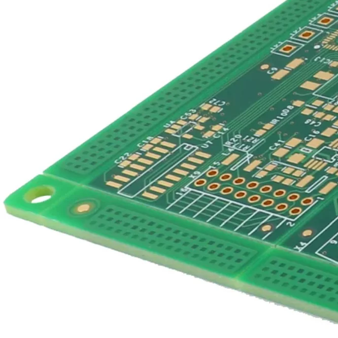
Turning an electronic design into a reliable physical product requires careful planning before production begins. A printed circuit board (PCB) provides the mechanical foundation for electronic components and establishes the conductive pathways that allow them to communicate. Even a well-designed circuit can encounter manufacturing defects if its layout, material specifications, or production files are incomplete. Learning how to prepare a PCB board for manufacturing helps engineers reduce avoidable errors and improve the quality of the finished product.
PCB manufacturing preparation involves several connected activities, from developing the circuit schematic and arranging components to defining fabrication requirements and validating production data. Each stage must account for electrical performance, mechanical dimensions, material properties, assembly requirements, and the capabilities of the selected manufacturer.

What is the Process of Preparing a PCB Board for Manufacturing?
Preparing a PCB for production means converting an electronic design into a complete, verified set of manufacturing and assembly instructions. The process typically begins with circuit design and continues through layout verification, specification selection, file generation, manufacturability review, and prototype validation.
1. Create a Schematic
The schematic defines the electrical architecture of the circuit and serves as the starting point for PCB development. It identifies the components, pin connections, power distribution, ground networks, and signal relationships required for the board to function correctly.
Use Electronic Design Automation (EDA) Software: Create the circuit diagram with a suitable EDA tool. Assign appropriate component symbols, reference designators, and electrical connections, and ensure that pin assignments correspond to the selected components.
Perform Electrical Rule Checks: Run an Electrical Rule Check (ERC) to identify issues such as unconnected pins, conflicting power connections, or incorrect electrical pin usage. Review warnings carefully instead of assuming that every warning represents a confirmed design failure.
Validate Circuit Behavior: Where appropriate, simulate important circuit functions to evaluate expected voltage levels, timing, current flow, or other operating characteristics. Specialized simulation may also be necessary for high-speed signals, power electronics, and electromagnetic compatibility.
A verified schematic provides the electrical reference for the next stage and helps prevent connectivity errors from carrying into the PCB layout.
2. PCB Layout Design
After completing the schematic, translate the electrical connections into a physical board design. This stage determines component positions, board dimensions, copper routing, and the arrangement of conductive and insulating layers.
Select Suitable Components: Check component specifications, package dimensions, electrical ratings, availability, and lifecycle status. Choosing appropriate parts early can reduce sourcing difficulties and avoid footprint changes later.
Choose PCB Design Software: Tools such as Altium Designer, KiCad, and EAGLE support component placement, trace routing, layer management, and design verification. Select a platform that meets the project's complexity and documentation requirements.
Optimize Component Placement: Position components according to their electrical functions, thermal characteristics, and mechanical constraints. Place decoupling capacitors close to the relevant IC power pins where practical, maintain separation between sensitive signals and noisy circuits, and ensure that connectors align with the intended enclosure.
Route Copper Traces Carefully: Establish trace widths and spacing based on current capacity, voltage requirements, impedance constraints, and the manufacturer's capabilities. High-speed or high-current designs may require additional calculations and specialized layout techniques.
Run Design Rule Checks: Use Design Rule Check (DRC) tools to identify clearance violations, insufficient trace widths, unconnected nets, and other layout problems. Confirm that the selected design rules reflect the actual fabrication and assembly requirements.
A well-constructed PCB layout should satisfy electrical and mechanical requirements while remaining practical to fabricate, assemble, inspect, and maintain.
3. Determine Manufacturing Standards
Before generating the final production package, define the physical construction and material specifications of the PCB. These decisions affect performance, manufacturing complexity, board durability, and overall cost.
Determine the Layer Count: Choose a single-layer, double-layer, or multilayer construction according to circuit complexity, routing density, signal integrity, and space limitations. Multilayer designs can accommodate more connections within a compact area but generally require additional manufacturing steps.
Select Appropriate Vias: Determine whether through-hole, blind, or buried vias are needed to connect copper layers. Via dimensions, aspect ratio, spacing, and placement must comply with the fabricator's process capabilities. Thermal management should be addressed through the complete copper and board design rather than via placement alone.
Choose the Substrate Material: FR-4 is widely used for general-purpose PCBs, while high-Tg laminates and specialized low-loss materials may be suitable for demanding thermal or high-frequency applications. Material selection should reflect the electrical, thermal, and mechanical requirements of the product.
Specify Board Thickness and Copper Weight: Define the finished board thickness and copper thickness according to the design requirements. Common copper weights include 1 oz and 2 oz per square foot, but the appropriate choice depends on current capacity, trace geometry, thermal performance, and manufacturing constraints.
Define Additional Fabrication Requirements: Specify the surface finish, solder mask, silkscreen, impedance control, board-edge requirements, and dimensional tolerances where applicable. Include any special requirements that could affect the production process or final inspection.
Confirm these specifications with the PCB manufacturer before finalizing the design, especially when the board uses specialized materials, fine-pitch components, or demanding electrical tolerances.
4. Creating Manufacturing Files
PCB manufacturers rely on accurate production data to fabricate the bare board and, when required, assemble the electronic components. The manufacturing package should contain all the information necessary to reproduce the intended design without ambiguity.
Gerber Files: Export the required copper, solder mask, silkscreen, and other applicable fabrication layers. Include the board outline in the format and manner requested by the manufacturer. Alternative formats, such as ODB++ or IPC-2581, may be accepted depending on the production workflow.
Drill Files: Provide NC drill data that defines the locations and sizes of plated and non-plated holes. Include any additional drilling or routing information requested by the fabricator.
Bill of Materials (BOM): Prepare a complete component list containing reference designators, manufacturer part numbers where applicable, values, quantities, package information, and approved alternatives if substitutions are permitted.
Pick-and-Place File: Supply component placement coordinates, rotation angles, reference designators, and side information in the manufacturer's preferred format. These data support automated component placement during assembly.
Assembly Drawings: Include clear illustrations showing component locations, polarity, orientation, and other relevant assembly details. Assembly drawings are particularly useful when a board includes connectors, mechanical parts, or components that require special handling.
Fabrication Notes and Stack-Up Information: Document the layer arrangement, material type, finished thickness, copper weight, surface finish, impedance requirements, and other critical specifications when these details are not fully defined elsewhere.
Gerber files and drill data are primarily used for PCB fabrication, whereas the BOM, pick-and-place data, and assembly drawings support component assembly. Review the manufacturer's file checklist to ensure the complete package is consistent and ready for production.

5. Design for Manufacturability (DFM) Confirmation
Design for Manufacturability (DFM) review evaluates whether a PCB can be produced reliably using the selected manufacturer's processes and capabilities. Completing this review before ordering boards helps uncover design problems that may otherwise result in delays, rework, or additional expenses.
Inspect Exported Manufacturing Files: Open the exported data in a Gerber viewer, such as KiCad GerbView or another compatible tool. Verify the board outline, copper patterns, drill locations, solder mask openings, and layer alignment.
Check Silkscreen Placement: Confirm that component labels and markings are readable and do not obscure exposed pads, mounting holes, or other critical features. Follow the manufacturer's minimum text and line-width requirements.
Review Pad Geometry and Clearances: Ensure that pad dimensions, solder mask clearances, conductor spacing, and copper-to-edge distances comply with the selected fabrication process and assembly requirements.
Confirm Drill and Routing Constraints: Check hole sizes, annular rings, via structures, and routed features against the fabricator's capabilities. Special structures may require explicit approval before production.
Validate Assembly Compatibility: Review component spacing, polarity markings, package orientation, and accessibility for soldering and inspection. Fine-pitch packages and unusual component geometries may require additional checks.
Resolve Manufacturing Feedback: Share the design package with the selected manufacturer for review where appropriate. Address identified issues and regenerate the files after any design changes.
A successful DFM review does not replace electrical verification, but it helps establish whether the design can be manufactured and assembled as intended.
6. Test and Programming Equipment
Some PCB projects require dedicated fixtures, test points, or programming interfaces to verify performance during production. These requirements should be considered during the design stage rather than added after the board has been finalized.
Define the Test Strategy: Identify which electrical functions must be verified, such as power input, signal communication, current consumption, and key circuit outputs.
Add Accessible Test Points: Provide suitable contact locations for probes, automated test fixtures, or in-circuit testing when required. Their positions should not interfere with components, connectors, or the enclosure.
Plan Programming Interfaces: If the PCB contains a microcontroller, programmable logic device, or other configurable component, determine how firmware or configuration data will be loaded. Include the required connectors, pads, or interface signals.
Consider Functional Test Fixtures: Products requiring repeatable production testing may benefit from a custom fixture or automated test setup. Ensure the board can be positioned securely and that relevant signals are accessible.
Document Test Requirements: Provide the manufacturer or assembly partner with test procedures, acceptance criteria, programming instructions, and any necessary configuration information.
Proper test planning helps identify electrical or assembly defects before products are shipped and can improve consistency across production batches.
7. Choosing a PCB Manufacturer
Once the design and production files have been prepared, select a manufacturer whose capabilities match the technical requirements and expected production volume. The lowest quotation is not necessarily the best option if the supplier cannot reliably meet the required tolerances, material specifications, or delivery schedule.
Evaluate Technical Capabilities: Check the manufacturer's supported layer count, minimum trace width and spacing, drilling capabilities, material options, surface finishes, and controlled-impedance services if needed.
Review Quality Management and Compliance: Ask about relevant quality systems, inspection processes, and certifications applicable to the product and target market. ISO, UL, and IPC-related requirements serve different purposes, so verify the specific qualification needed for the project.
Compare Cost and Lead Time: Consider prototype pricing, tooling charges, production quantities, shipping, and the time required for fabrication and assembly. Confirm whether the quoted schedule includes engineering review and any necessary testing.
Discuss Manufacturing Requirements: Share the fabrication package and explain special requirements, including stack-up, impedance, materials, testing, and assembly instructions. Resolve technical questions before authorizing production.
Review Communication and Support: A responsive manufacturing partner can help identify manufacturability concerns and clarify documentation issues before they affect the delivery schedule.
Selecting a suitable manufacturer establishes a clearer path from PCB design to production and helps ensure that the finished boards meet the project's requirements.
8. Prototype Order
A prototype run provides an opportunity to validate the design before committing to larger production quantities. Even when a layout passes automated checks, physical testing may reveal problems related to assembly, electrical performance, component fit, or operating temperature.
Order a Representative Prototype: Use the same essential materials, layer structure, and fabrication specifications intended for production whenever practical. This makes the results more relevant to the final product.
Verify Mechanical Fit: Check board dimensions, mounting holes, connector alignment, enclosure clearance, and component height against the intended assembly.
Perform Electrical Tests: Confirm power distribution, connectivity, signal behavior, and key functional requirements. Use suitable measurement equipment and test procedures for the circuit's operating conditions.
Evaluate Thermal Performance: Monitor components and board areas that may experience elevated temperatures during normal operation or demanding workloads. Compare results with component specifications and the product's thermal requirements.
Inspect Assembly Quality: Examine solder joints, component placement, polarity, and potential manufacturing defects. Additional inspection methods may be appropriate for fine-pitch packages or complex multilayer designs.
Refine the Design Before Mass Production: Document identified problems, implement necessary changes, and repeat relevant verification tests. Keep manufacturing files synchronized with the approved design revision.
Prototype validation helps reduce the risk of costly production changes and provides evidence that the board can meet its intended requirements.
Benefits of Proper PCB Preparation
Investing time in PCB manufacturing preparation improves coordination between design, fabrication, assembly, and testing. A complete and verified production package gives the manufacturer clearer instructions and helps prevent avoidable mistakes.
Fewer Manufacturing Errors: Accurate footprints, verified connectivity, and complete production files reduce the likelihood of incorrect drilling, routing problems, assembly confusion, and other preventable defects.
Improved Production Efficiency: Clear specifications and early DFM reviews help manufacturers identify concerns before fabrication begins. This can reduce clarification cycles, redesign work, and unnecessary production delays.
Better Cost Control: Resolving design issues before ordering boards helps avoid repeated prototype runs, material waste, and expensive modifications after production has started.
More Reliable Product Performance: Appropriate materials, carefully planned routing, and thorough prototype testing help the PCB meet its electrical, thermal, and mechanical requirements.
Smoother Scaling to Mass Production: Consistent documentation, revision control, and validated test procedures make it easier to transfer a successful prototype into repeatable manufacturing.
Conclusion
Preparing a PCB board for manufacturing requires a systematic process that connects circuit design with practical fabrication and assembly requirements. From creating a verified schematic and optimizing the layout to defining materials, generating production files, completing DFM checks, and validating prototypes, every stage contributes to the quality of the finished product.
Understanding how to prepare a PCB board for manufacturing helps engineers reduce design errors, improve communication with suppliers, and make informed decisions about materials, costs, and production methods. Careful preparation is especially important for complex multilayer boards, high-speed circuits, and products that must meet demanding reliability or compliance requirements.