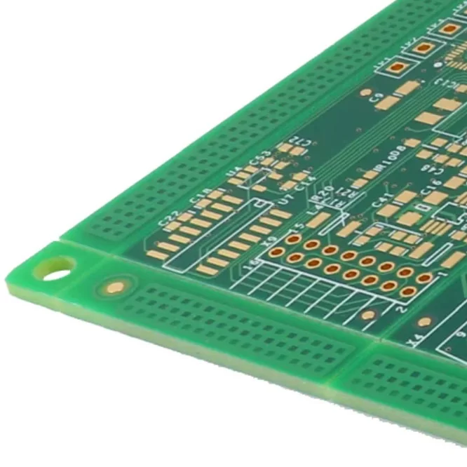
A printed circuit board (PCB) serves as the foundation of an electronic assembly, supporting components and providing conductive paths for power and signal transmission. It typically consists of an insulating substrate combined with patterned copper layers. Although modern manufacturing processes have improved PCB consistency and reliability, defects can still develop because of electrical overstress, mechanical damage, component failure, material imperfections, or assembly errors.
Not every PCB fault requires replacing the entire board. Depending on the location and severity of the damage, a technician may be able to restore functionality by repairing a broken trace, replacing a defective component, or correcting a soldering defect. Knowing how to fix PCB board problems begins with accurate diagnosis, suitable repair tools, and a clear understanding of the board's construction.

Essential Tools for PCB Board Repair
Having the right tools available before starting a repair helps improve accuracy and reduces the risk of causing additional damage. PCB repair typically involves three stages: identifying the fault, carrying out the repair, and verifying that the circuit operates correctly. Each stage requires equipment suited to the task.
The following tools are commonly used for soldering, desoldering, inspection, and electrical testing.
Basic Soldering Tools
Soldering Iron: A temperature-controlled soldering iron supplies the heat needed to remove components, reflow existing solder, and establish new electrical connections. Select a suitable tip size for the component and pad geometry.
Desoldering Pump: This tool uses suction to remove molten solder from through-hole joints. It is particularly useful when clearing plated holes before removing connectors or other leaded components.
Solder Braid: Also known as solder wick, this woven copper material absorbs molten solder. It helps remove excess solder, clear bridges between adjacent pads, and prepare joints for rework.
Solder Wire: Solder wire is used to create or restore electrical connections during component installation and joint repair. The alloy and diameter should be compatible with the assembly and the required process.
Flux Pen: Flux improves solder wetting by helping remove surface oxides during heating. Applying an appropriate amount can make soldering more consistent and reduce the likelihood of poorly formed joints.
Inspection and Diagnostic Tools
Before attempting a repair, technicians need to determine whether the problem originates from a component, a conductive trace, a solder joint, or another part of the circuit.
Multimeter: A digital multimeter measures voltage, resistance, and continuity. It can help identify open connections, investigate suspected shorts, and check component values when the component is isolated or the circuit conditions allow reliable measurement.
Oscilloscope: An oscilloscope displays electrical signals over time, helping technicians examine waveform shape, timing, noise, and signal integrity. It is useful when a PCB powers on but does not behave as expected.
Luxo Lamp or Microscope: Magnified visual inspection can reveal cracked solder joints, lifted pads, damaged traces, component discoloration, and other defects that are difficult to see with the naked eye.
ESD Mat and Wrist Strap: Electrostatic discharge can damage sensitive electronic devices without leaving visible evidence. An appropriate ESD workstation and properly grounded wrist strap help protect components during handling and repair.
Advanced Repair Equipment
More complex PCB assemblies may require specialized equipment, especially when working with fine-pitch components, hidden solder joints, or high-density layouts.
Reflow Oven: A reflow oven follows a controlled thermal profile to melt solder paste and form connections across assembled surface-mount components. It is primarily used for assembly and controlled rework rather than routine single-joint repairs.
BGA Rework Station: Ball Grid Array (BGA) packages have solder connections beneath the component body, making them difficult to rework with conventional tools. A dedicated BGA station provides controlled heating, often from above and below, to support component removal and replacement.
X-ray Inspection System: X-ray inspection reveals solder joints and internal structures hidden beneath packages such as BGAs. It helps identify issues including voids, bridging, and other defects that cannot be confirmed through ordinary visual inspection.
The equipment required depends on the fault and the PCB design. Simple repairs may need only a multimeter and soldering tools, whereas multilayer boards and advanced packages may require professional diagnostic and rework systems.

Common PCB Board Repair Methods
PCB repair should begin with a systematic diagnosis rather than replacing parts based on appearance alone. Disconnect the power supply before handling the board, allow stored energy to discharge safely, and follow appropriate ESD precautions. For powered measurements, use suitable procedures and equipment to avoid electrical hazards.
The following methods explain how to fix PCB board faults commonly encountered during electronic assembly, maintenance, and troubleshooting.
1. Trace Repair
Copper traces carry electrical signals and power between PCB components. A trace may become damaged because of excessive heat, mechanical scratches, corrosion, manufacturing defects, or previous repair work. When the conductive path is interrupted, the circuit may stop functioning or become intermittent.
Continuity Testing. Start by identifying the suspected damaged trace and checking its electrical path with a multimeter. Perform continuity testing with the board unpowered and isolated from relevant circuit paths where necessary. Compare the results with the circuit layout to determine whether the connection is open or affected by other components in parallel.
Prepare the Traces. Carefully remove a small amount of solder mask from the damaged trace ends to expose clean copper. Avoid cutting into the conductive layer or damaging nearby traces. Clean the repair area using a compatible cleaning method and allow it to dry before applying flux.
Solder the Jumper. Select a jumper wire appropriate for the circuit's current, voltage, and mechanical requirements. Apply flux to the exposed copper and solder one end of the wire to each side of the break. Keep the wire as short and secure as practical, particularly for high-speed or sensitive signal paths, where the added connection may affect electrical performance.
Protect the Repaired Trace with a Solder Mask. After the joint has cooled, inspect the solder connections and verify electrical continuity. Once the repair is confirmed, apply a suitable insulating coating or solder mask repair material to protect the exposed copper. Ensure the coating is compatible with the board and does not cover contact points that must remain accessible.
A jumper-wire repair is suitable for certain accessible outer-layer traces. Damage to internal layers, high-current paths, controlled-impedance signals, or safety-critical circuits may require specialized repair procedures or replacement of the PCB.
2. Component Replacement
A PCB component may need replacement when it has failed electrically, suffered physical damage, overheated, or no longer meets the circuit's requirements. Capacitors, diodes, resistors, transistors, and integrated circuits are among the components that may require rework. The removal and installation procedure depends on whether the part uses through-hole leads or surface-mount terminals.
Power off the PCB. Disconnect the board from all power sources and discharge capacitors using an appropriate procedure. Never assume a capacitor is safe simply because the equipment has been switched off. Use ESD protection when handling sensitive devices, and consult the circuit documentation before working on high-voltage assemblies.
Identify the Fault. Inspect the board for cracked packages, leakage, discoloration, damaged terminals, or abnormal solder joints. Use a multimeter or other suitable test equipment to evaluate the suspected component. Measurements taken in-circuit may be affected by surrounding components, so isolation or additional testing may be necessary to confirm the diagnosis.
Remove the Component. Choose a removal method that matches the component package and PCB construction. Avoid applying excessive force, as this can lift copper pads or damage plated holes.
Through-hole Components. Heat each solder joint on the underside of the board until the solder melts. Remove the molten solder with a desoldering pump or solder braid. Once the leads are free, withdraw the component gently. If a lead remains stuck, reheat the joint and clear any residual solder rather than pulling harder.
Surface Mount Components. Apply a suitable amount of flux to the solder joints. For small components, a soldering iron may be sufficient; packages with multiple terminals may require hot-air rework equipment. Heat the joints evenly and lift the component only after the solder has melted. Protect nearby parts from heat and avoid excessive airflow that could displace small components.
Solder the New Component. Verify that the replacement part matches the required electrical specifications, package size, and temperature rating. Check polarity and pin orientation before soldering, as incorrect placement can cause circuit failure or component damage.
Through-hole Components. Insert the component leads into the correct holes and confirm that the part sits in the intended position. Solder each lead using sufficient heat and solder to create a reliable joint. Trim excess lead length where appropriate, then inspect the joints for incomplete wetting, excess solder, or unintended bridges.
Surface Mount Components. Apply solder paste or flux as appropriate for the repair method, then align the replacement component accurately with its pads. Solder the terminals using a suitable iron or controlled rework process. For fine-pitch packages, inspect the joints under magnification and check for bridging or misalignment before proceeding.
Verify the Replaced Component. Examine the repaired area and use a multimeter to check relevant connections, polarity, and potential shorts. Where necessary, perform additional electrical measurements or functional testing under controlled conditions. A successful component replacement should restore the intended function without introducing new faults.
3. Soldering Defects
Soldering defects can interrupt electrical connections or create unintended conductive paths between adjacent pads. Some problems can be corrected with localized rework, while others may indicate wider issues with the assembly process. Identify the defect first, then select the appropriate repair technique.
Cold Solder Joint. A cold or poorly wetted solder joint may appear dull, irregular, or cracked, although appearance alone is not sufficient to confirm the defect. Such joints can result from inadequate heating, contaminated surfaces, or unsuitable soldering conditions. Apply flux if appropriate, reheat the joint until the solder wets the pad and terminal correctly, and add a small amount of compatible solder when needed. Inspect the finished joint and check electrical continuity.
Solder Bridges. A solder bridge forms when excess solder connects two or more pads that should remain electrically separate. This can create a short circuit and prevent the device from operating correctly. Apply flux and use solder braid or a suitable desoldering tool to remove the excess solder. Rework the affected joints with controlled heat, then inspect the spacing between pads and test for unintended electrical connections before powering the board.
Tombstoning. Tombstoning is a surface-mount assembly defect in which one end of a small component lifts from its pad during reflow, leaving the component standing at an angle. It is often associated with uneven wetting forces, imbalanced pad heating, or differences in solder paste deposition. For rework, remove the affected component if necessary, clean and prepare the pads, and reinstall a suitable replacement or the original part if it remains serviceable. Apply solder paste or solder as appropriate, position the component accurately, and use a controlled reflow or soldering process. For recurring tombstoning, review the stencil design, pad geometry, component placement, and reflow profile rather than relying solely on individual repairs.
Conclusion
Repairing a PCB successfully requires accurate fault identification, suitable tools, and careful control of heat and handling. Broken traces may be restored with an appropriate jumper connection, defective components can often be replaced, and soldering problems may be corrected through targeted rework. However, not every damaged board is suitable for repair, particularly when internal layers or critical electrical structures are affected.