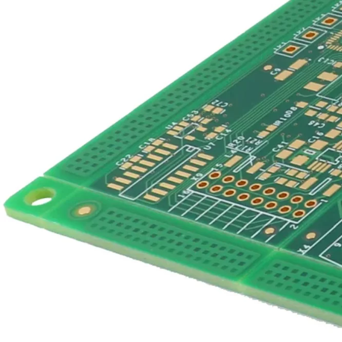
Modern electronic technology continues to evolve, making devices smaller, more powerful, and increasingly versatile. Smartphones, computers, medical instruments, automotive systems, and industrial control equipment all rely on carefully designed electronic circuits to perform their functions. Behind these technologies is a fundamental component that connects electronic parts and enables them to work together: the printed circuit board (PCB).
A PCB provides a structured platform for mounting electronic components and establishing electrical connections between them. Its design and manufacturing quality directly influence the performance, stability, and service life of the final product. Understanding how to make PCB board products involves more than arranging copper traces; it requires coordinated design, material selection, precision fabrication, and quality control.

What is PCB?
A printed circuit board (PCB) is an electronic substrate that mechanically supports components and electrically connects them through patterned copper traces, conductive pads, and, where required, plated holes or vias. Depending on the intended application, a PCB may contain one or multiple conductive layers separated by insulating materials.
The substrate provides structural support, while the copper circuitry creates the paths through which power and electrical signals travel. Common materials include FR-4 glass-reinforced epoxy laminate, as well as specialized flexible substrates for applications requiring bending or compact packaging.
PCB design must account for several technical factors, including trace width, electrical clearance, impedance control, heat dissipation, and electromagnetic compatibility. These requirements become particularly important in high-speed electronics, power systems, and multilayer designs. A clear understanding of these fundamentals provides a strong starting point for learning how to make PCB board assemblies that meet their intended electrical and mechanical requirements.
What are the Different Types of PCBs?
PCB structures vary according to the number of copper layers, the substrate material, and the mechanical requirements of the application. Selecting the appropriate construction helps balance circuit complexity, manufacturing cost, reliability, and available installation space.
Single-Sided PCB. A single-sided PCB contains copper circuitry on only one side of the insulating substrate. Its straightforward structure makes it suitable for relatively simple circuits, including basic power supplies, lighting products, and household electronic devices. With fewer processing requirements, this board type is often an economical option for high-volume production.
Double-Sided PCB. A double-sided PCB features conductive copper layers on both sides of the substrate. Plated through-holes connect the two layers, allowing designers to route more signals within a limited board area. This construction is widely used in control systems, communication equipment, and electronic products that require greater circuit density than a single-sided design can provide.
Multi-layered PCB. A multilayer PCB consists of three or more conductive layers bonded together with insulating materials. Electrical connections between selected layers are established through vias. Multilayer construction supports complex routing, power distribution, and signal integrity requirements, making it common in servers, networking hardware, medical electronics, and advanced industrial equipment.
Rigid PCB. A rigid PCB uses a mechanically stable substrate, commonly FR-4, that maintains its shape during installation and operation. Depending on the design, it can incorporate one or multiple copper layers. Rigid boards are widely used in computers, appliances, automotive electronics, and other products where a stable mounting platform is required.
Flexible PCB. A flexible PCB is manufactured with bendable insulating materials, typically polyimide, and thin copper conductors. Its ability to conform to curved surfaces or fit into narrow spaces makes it useful in cameras, wearable devices, display modules, and compact electronic assemblies. Flexible designs can also reduce the need for cables and connectors in certain applications.
Rigid–flex PCB. A rigid-flex PCB combines rigid circuit sections with flexible interconnecting areas in a single integrated structure. This arrangement supports three-dimensional packaging while reducing the number of separate connectors and cables. Rigid-flex technology is particularly valuable in aerospace equipment, medical devices, and compact electronics where space, weight, and connection reliability are important.
How to Make a PCB Board?
Commercial PCB fabrication involves a sequence of controlled processes that transform circuit design data and raw laminate materials into a finished board. The exact workflow depends on the layer count, material system, feature dimensions, and required performance. The following stages explain how PCB manufacturers typically produce rigid multilayer boards, with some processes adapted for simpler constructions.
Design (Schematics and Layout). PCB production begins with an electrical schematic that defines components, signal connections, and circuit relationships. Engineers then use Electronic Design Automation (EDA) software to create the physical board layout, assigning component positions and routing copper traces. Before fabrication, the design should be checked for electrical connectivity, spacing, manufacturability, and thermal considerations. Design rule checks and design-for-manufacturing reviews help identify potential problems before they become costly production defects.
Core and Inner Layer Processing. For multilayer boards, copper-clad laminate panels are prepared for inner-layer circuit formation. A photoresist coating is applied, and the required circuit pattern is transferred through direct imaging or another suitable imaging process. The panel is then developed and etched to remove unwanted copper, leaving the intended conductive traces. Inspection verifies the pattern and checks for opens, shorts, or other defects before the layers proceed to lamination.
Lamination. Once the inner layers are prepared and inspected, they are aligned with insulating prepreg sheets and other required materials. Heat and pressure are applied in a controlled lamination cycle to bond the stack into a unified panel. Precise layer registration, temperature control, pressure, and resin flow are essential for maintaining board thickness and preventing separation between layers. This stage is especially important for multilayer designs with tight alignment tolerances.
Drilling. Holes are created to accommodate component leads, mounting hardware, and electrical connections between conductive layers. CNC drilling equipment follows programmed drill data to maintain hole position and diameter. Mechanical drilling is commonly used for standard through-holes, while laser drilling may be selected for small microvias in high-density interconnect designs. Accurate drilling helps prevent damaged pads, poor interconnections, and assembly difficulties.
Plating and Outer Layer Processing. After drilling, the hole walls are prepared and plated with copper to establish electrical connections between the relevant layers. The outer copper layers are then patterned using imaging and etching processes similar to those used for inner layers. These operations form the external traces, component pads, and other conductive features. Depending on the board design, additional plating and patterning steps may be required to achieve the specified copper thickness and conductor geometry.
Solder Masking. A solder mask is applied over selected areas of the copper circuitry to help protect the board from oxidation, contamination, and accidental solder bridging. Openings are retained over component pads and other locations that must remain accessible for soldering. Liquid photoimageable solder mask is widely used because it supports detailed patterns and consistent coverage. Proper coating, exposure, development, and curing help ensure reliable adhesion and accurately defined openings.
Silk Screening. Legend printing adds useful identification information to the PCB surface, including component reference designators, polarity indicators, connector labels, logos, and manufacturing codes. These markings assist technicians during assembly, inspection, testing, and maintenance. Depending on the production requirements, manufacturers may use screen printing, direct legend printing, or other suitable marking techniques. Clear and correctly positioned legends improve usability without interfering with solder pads or other critical features.
Surface Finishing. Exposed copper pads require a suitable surface finish to protect them during storage and provide reliable solderability during assembly. Common options include ENIG (Electroless Nickel Immersion Gold), HASL (Hot Air Solder Leveling), and OSP (Organic Solderability Preservative). Each finish has different characteristics relating to cost, flatness, shelf life, and application suitability. The appropriate choice depends on component pitch, assembly requirements, environmental conditions, and the intended service life of the electronic product.

What are the Common Issues during PCB Fabrication?
Even when a PCB design is well prepared, manufacturing variations can introduce defects that affect electrical performance, mechanical stability, or assembly yield. Identifying the causes of these problems and implementing suitable process controls are essential parts of producing reliable circuit boards.
Design-Related Issues. Inadequate trace spacing, incorrect pad dimensions, unsuitable drill sizes, and insufficient thermal planning can make a design difficult to manufacture or operate reliably. Poorly controlled impedance or inappropriate stack-up selection may also affect signal performance in demanding applications. Engineers can reduce these risks by completing design rule checks, reviewing fabrication capabilities, and conducting design-for-manufacturing assessments before production begins.
Plating Issues. Inconsistent copper deposition, incomplete hole coverage, and plating voids can weaken electrical connections between layers. These defects may increase resistance or cause intermittent failures, especially under thermal or mechanical stress. Manufacturers should maintain appropriate chemical conditions, monitor plating parameters, inspect hole quality, and verify copper thickness against the required specifications. Reliable process control is particularly important for boards with dense via structures and demanding current requirements.
Delamination. Delamination occurs when bonded PCB layers or material interfaces separate. It may result from unsuitable lamination conditions, moisture absorption, material incompatibility, or excessive thermal stress during later processing. Separation can compromise structural integrity and may damage electrical connections. Prevention includes proper material storage, moisture management, controlled lamination cycles, and compliance with the thermal requirements of the selected laminate system.
Board Warpage. PCB warpage refers to unwanted bending or twisting that can interfere with automated component placement, soldering, and enclosure assembly. Uneven copper distribution, differences in material expansion, panel design, and thermal processing can contribute to this problem. Manufacturers can help control warpage through balanced copper layouts, suitable material selection, optimized panel arrangements, and carefully managed lamination and soldering profiles. Board flatness should be checked against the applicable specifications.
Drilling Defects. Poor hole positioning, excessive burrs, rough hole walls, and damaged pads can compromise electrical connections or prevent components from fitting correctly. Drill wear, incorrect drilling parameters, inadequate tool selection, and misaligned fabrication data may contribute to these defects. Preventive measures include maintaining drill tools, using verified drill files, controlling machine parameters, and inspecting hole dimensions and quality. For demanding multilayer boards, appropriate inspection of plated holes is also necessary to confirm interconnection reliability.
Conclusion
Producing a reliable PCB requires a coordinated process that begins with accurate circuit design and continues through material preparation, circuit imaging, lamination, drilling, plating, solder mask application, surface finishing, and inspection. Each stage contributes to the board's electrical performance, mechanical stability, and compatibility with the assembly process.