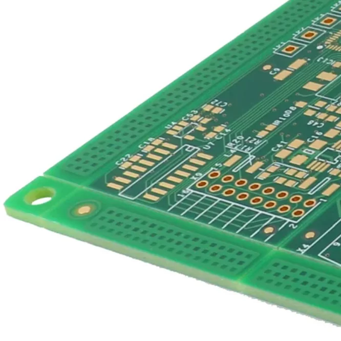
Building a circuit on a breadboard is an excellent way to test a design, but it is only the first stage of electronics development. If you want a circuit that is durable, compact, and suitable for long-term use, transferring the design onto a Printed Circuit Board (PCB) is the next logical step. For electronics enthusiasts, students, and engineers, learning how to etch a PCB board is one of the most practical skills for creating custom circuit boards without relying on professional manufacturing services.
PCB etching is the process of selectively removing unwanted copper from a copper-clad laminate, leaving only the conductive traces that form the circuit. The copper traces are protected by a printed layout, while the exposed copper is dissolved using a chemical etching solution. Once the etching process is complete, the remaining copper forms the electrical pathways that connect the electronic components.

Methods for Transferring PCB Layouts
Before any copper can be removed, the PCB layout must first be transferred onto the copper surface. The transferred pattern acts as a protective mask, ensuring that only unwanted copper is dissolved during etching.
Several techniques are commonly used to transfer PCB designs.
The toner transfer method is the most popular option for hobbyists because it requires only basic equipment such as a laser printer and a household iron.
The photoresist method produces higher precision and is suitable for fine-pitch circuits, but it requires UV exposure equipment and photosensitive boards.
For advanced users, CNC engraving or laser engraving machines can directly remove unwanted copper or create precise masks without using transfer paper.
Among these methods, the toner transfer process offers the best balance between simplicity, cost, and reliability, making it the preferred choice for beginners learning how to etch a PCB board.
Toner Transfer Method for PCB Etching
The toner transfer process converts a digital PCB layout into a physical copper pattern using heat. Although the procedure is straightforward, achieving clean and accurate traces requires careful preparation.
Materials and Tools
Before starting, prepare the following materials:
l Copper-clad PCB board
l Laser printer
l Glossy transfer paper or dedicated toner transfer paper
l Household iron or laminator
l Plastic tray
l Selected PCB etching solution
l Fine sandpaper or steel wool
l Acetone or isopropyl alcohol
l Safety gloves, goggles, and protective clothing
Once everything is ready, the PCB fabrication process can begin.
Step 1: Design and Print Your PCB Layout
Start by designing the circuit using PCB software such as KiCad, EasyEDA, or Eagle.
After completing the layout, export the PCB artwork at a true 1:1 scale. If transferring the top copper layer, remember to mirror the design before printing so it appears correctly after transfer.
Print the layout using a laser printer, since laser toner melts and bonds to copper during heating. Inkjet printers cannot be used because their ink does not transfer properly.
For the highest-quality transfer, select the printer's highest resolution and disable automatic scaling.
Step 2: Prepare the Copper Boards
A clean copper surface is essential for successful toner adhesion.
Cut the copper-clad board to the required dimensions and smooth the edges if necessary.
Use fine sandpaper or steel wool to remove oxidation, fingerprints, and surface contaminants. Continue polishing until the copper has a bright, even appearance.
Finally, wipe the surface with acetone or high-purity isopropyl alcohol to remove grease and dust. Avoid touching the cleaned copper with bare hands afterward.
Proper preparation greatly improves the success rate when learning how to etch a PCB board.
Step 3: Transfer the Toner
Place the printed PCB artwork face-down on the cleaned copper surface.
Apply consistent heat using a household iron or laminator. Moderate pressure should be maintained while slowly moving the iron across the paper to ensure the toner melts evenly onto the copper.
Heating generally takes several minutes depending on board size and equipment.
After cooling, soak the board in warm water until the paper softens. Carefully peel away the paper, leaving only the toner image attached to the copper.
Inspect the transferred pattern carefully. Small defects can often be repaired using a permanent marker before etching begins.
Step 4: Etch the Board
Prepare a plastic container with the chosen PCB etching solution according to the manufacturer's recommendations.
Place the board into the solution with the copper surface facing upward whenever possible. Gentle movement or agitation helps fresh solution contact the exposed copper, improving etching speed and uniformity.
As the chemical reaction progresses, the exposed copper gradually dissolves while the toner protects the desired circuit traces.
When all unnecessary copper has disappeared, immediately remove the board and rinse it thoroughly with clean water to stop the reaction.
Careful observation during this stage is essential for achieving clean traces without over-etching.
Step 5: Clean and Finish the Board
Once etching has been completed, remove the remaining toner using acetone or a dedicated toner remover.
Inspect the copper traces for breaks, shorts, or incomplete etching. Minor defects may be repaired using conductive wire or additional solder during assembly.
If desired, apply a solder mask to protect the copper against oxidation and improve soldering performance.
Finally, drill component holes using the appropriate drill bits before assembling the electronic components.
At this point, your custom PCB is ready for soldering and functional testing.

Etching Solutions: Choosing the Right One
The quality and speed of PCB fabrication largely depend on the etching solution selected. Different chemicals offer different advantages depending on project requirements.
Etching Solution | Speed | Cleanliness | Availability | Advantages | Limitations |
Ferric Chloride | Medium | Stains easily | Widely available | Low cost, dependable, commonly used | Difficult cleanup and disposal |
Ammonium Persulfate | Medium | Very clean | Electronics suppliers | Transparent solution allows easy monitoring | Strong oxidizer that requires careful handling |
Cupric Chloride | Fast | Moderate | DIY preparation possible | Reusable and environmentally friendlier | Requires hydrochloric acid and proper ventilation |
Salt + Vinegar + Hydrogen Peroxide | Slow | Clean | Household materials | Very inexpensive and beginner-friendly | Slow reaction and unsuitable for fine traces |
Each solution has its own strengths, so selecting the right chemical depends on experience level, board complexity, and available equipment.
Which one should you choose?
For most first-time PCB makers, ferric chloride remains the easiest solution to obtain and delivers consistent results.
If cleaner operation is preferred, ammonium persulfate provides a transparent solution that allows the etching progress to be monitored more easily.
Experienced hobbyists often choose cupric chloride because it can be regenerated and reused multiple times, reducing chemical waste.
Household mixtures based on vinegar and hydrogen peroxide are useful for educational demonstrations but are generally too slow for complex PCB layouts with fine traces.
Choosing the appropriate etchant is an important part of mastering how to etch a PCB board efficiently.
Safety Tips for PCB Etching
Chemical safety should always be treated as a priority throughout the etching process.
Wear chemical-resistant gloves, safety goggles, and protective clothing whenever handling etching solutions.
Perform all chemical work in a well-ventilated workspace to avoid inhaling fumes generated during the reaction.
Use only plastic or glass containers, since metal containers may react with the chemicals.
Never prepare food or drink near the work area, and always keep children and pets away from the workspace.
Used etching chemicals should never be poured directly into household drains. Dispose of them according to local environmental regulations.
After completing the project, wash your hands thoroughly and clean all equipment before storage.
Safe working habits not only protect the operator but also improve the overall success of every DIY PCB project.