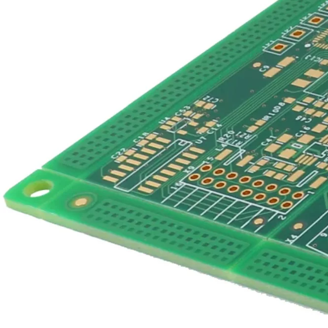
Printed Circuit Boards (PCBs) are the foundation of virtually every electronic product, from consumer electronics and industrial controllers to automotive systems and medical equipment. As electronic devices continue to become smaller, faster, and more intelligent, PCB designs have evolved from simple single-layer circuits into highly integrated multilayer boards containing thousands—or even millions—of electrical connections.
With increasing circuit density comes a greater possibility of manufacturing defects, assembly issues, or damage during operation. One of the most common and potentially destructive faults is a short circuit. A short circuit can interrupt normal circuit operation, damage electronic components, generate excessive heat, or even cause complete system failure. Therefore, understanding how to detect short circuit in PCB is an essential skill for engineers, technicians, and electronics manufacturers.

What is a Short Circuit and its Causes?
A short circuit occurs when two electrical points that should remain electrically isolated become unintentionally connected. Instead of following the intended circuit path, electrical current takes a lower-resistance route, often causing excessive current flow.
Depending on the location and severity of the fault, a short circuit may affect only a small section of the PCB or disable the entire electronic system.
Several factors can contribute to PCB short circuits.
Design errors are one of the earliest causes. Inadequate trace spacing, incorrect net assignments, overlapping copper pours, or layout mistakes can create unintended electrical connections before manufacturing even begins.
Manufacturing defects are another common source. Excess solder may bridge adjacent pads, pins, or traces during assembly, especially on fine-pitch surface-mount components. Improper solder mask application may also expose copper areas that accidentally become connected.
Incorrect component placement can also create shorts if leads contact neighboring pads or copper traces.
Environmental contamination is another risk factor. Moisture, conductive dust, metal particles, corrosion, or chemical residues deposited on the PCB surface may eventually create conductive paths between isolated circuits.
For multilayer PCBs, internal layer misalignment or manufacturing defects may produce hidden short circuits that are difficult to locate using conventional inspection methods.
Even during maintenance or repair, poorly installed jumper wires or incorrect soldering techniques may introduce new short circuits.
Understanding these causes is the first step toward mastering how to detect short circuit in PCB effectively.
Symptoms of a Short Circuit in the PCB
A PCB experiencing a short circuit usually exhibits abnormal electrical or thermal behavior before complete failure occurs.
One of the most noticeable symptoms is a device that refuses to power on or repeatedly resets during operation.
Power supplies may immediately enter protection mode or blow fuses because excessive current is being drawn by the shorted circuit.
Components near the fault often become unusually hot within seconds after power is applied. In severe cases, discoloration, smoke, or a burnt odor may appear.
Voltage regulators may output incorrect voltages, while processors, sensors, or communication modules may behave unpredictably.
Battery-powered devices often experience significantly reduced operating time because the short continuously consumes electrical energy.
Recognizing these warning signs allows technicians to begin troubleshooting before more extensive damage occurs.
Short Circuit Detection Techniques
Locating a short circuit requires a systematic approach. Depending on the PCB complexity and available equipment, technicians may combine several inspection methods to identify the exact fault location.
Visual Inspection
Visual inspection is always the recommended starting point.
Using adequate lighting and magnification, examine the PCB carefully for solder bridges, damaged copper traces, misplaced components, lifted pads, foreign metal particles, or burn marks.
A microscope or magnifying glass is especially useful when inspecting high-density surface-mount assemblies where tiny solder bridges may be invisible to the naked eye.
The PCB should also be inspected from multiple viewing angles because reflected light often reveals solder defects more clearly.
Although visual inspection cannot detect every hidden fault, it often identifies obvious assembly problems quickly without requiring specialized equipment.
Manual Testing
When visual inspection does not reveal the fault, electrical measurements provide the next level of diagnosis.
A digital multimeter set to continuity mode is one of the most useful tools for PCB troubleshooting.
Measure continuity between suspected nodes, power rails, and ground. If the meter produces a continuous beep where no electrical connection should exist, a short circuit is likely present.
Resistance measurements provide additional information. Extremely low resistance between power and ground often indicates a direct short.
Technicians frequently isolate different circuit sections by removing components one at a time until the abnormal resistance disappears, helping narrow down the fault location.
Manual testing remains one of the most practical methods for learning how to detect short circuit in PCB.
Automation Testing
Large-scale PCB manufacturing relies heavily on automated inspection systems to improve efficiency and consistency.
Automated Optical Inspection (AOI) compares high-resolution images of manufactured PCBs with reference design files. Advanced image processing algorithms identify solder bridges, missing components, polarity errors, and many visible short circuits.
In-Circuit Testing (ICT) uses a bed-of-nails fixture to contact hundreds or thousands of PCB test points simultaneously. Automated measurements verify continuity, resistance, component values, and electrical connectivity throughout the circuit.
Flying Probe Test systems offer another solution for low-volume manufacturing by electrically testing PCB connections without dedicated fixtures.
These automated technologies dramatically improve production quality while reducing inspection time and human error.
Advanced Testing Methods
Some PCB faults cannot be located using ordinary inspection techniques, especially in complex or high-density electronic assemblies.
Infrared thermal imaging cameras help identify abnormal heat generated by excessive current flowing through the shorted area. Even when the physical defect cannot be seen directly, the resulting heat pattern often reveals its location.
Current tracing equipment detects magnetic fields generated by electrical current, allowing technicians to follow the current path until the short is located.
Time Domain Reflectometry (TDR) is another advanced diagnostic technique. High-speed electrical pulses travel through PCB traces, and reflections caused by impedance changes help identify faults such as opens or short circuits within complex transmission lines.
These specialized methods are widely used in aerospace, telecommunications, automotive electronics, and other industries requiring advanced diagnostic capabilities.
Detection in Multilayer PCBs
Multilayer PCBs present unique troubleshooting challenges because many copper traces are completely enclosed within the board.
Since internal layers cannot be inspected visually, X-ray inspection is commonly used to detect hidden solder bridges, via defects, internal copper shorts, or misplaced components beneath BGAs and other complex packages.
Computed Tomography (CT) scanning provides even more detailed three-dimensional images of multilayer PCB structures.
In rare situations involving severe product failures or forensic analysis, engineers may perform layer-by-layer destructive analysis to expose internal copper connections. Although destructive, this technique provides valuable information for failure analysis and future design improvements.
Understanding these specialized methods is an important part of mastering how to detect short circuit in PCB for advanced electronic products.

Prevention of Short Circuits in PCB Design and Production
Preventing short circuits is far more efficient than repairing them after production.
PCB designers should maintain adequate spacing between copper traces according to industry design standards and perform comprehensive Design Rule Checks (DRC) and Electrical Rule Checks (ERC) before releasing manufacturing files.
High-quality solder mask application helps prevent accidental solder bridges during assembly.
Manufacturers should maintain strict process control throughout PCB fabrication and SMT assembly, including stencil printing, component placement, reflow soldering, and inspection.
Clean manufacturing environments minimize conductive contamination, while proper storage reduces moisture absorption and oxidation.
Finally, comprehensive electrical testing before shipment ensures that defective boards are identified before reaching customers.
By combining careful design practices with effective quality control procedures, manufacturers can significantly reduce the likelihood of short circuits while improving long-term PCB reliability.