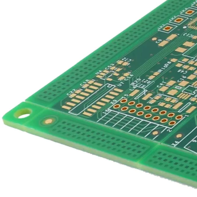
As electronic devices become smaller, faster, and more sophisticated, printed circuit board (PCB) manufacturing continues to evolve. Modern fabrication techniques rely on precise equipment, advanced materials, and carefully controlled chemical treatments to meet increasingly demanding requirements for electrical performance and product reliability. Alongside improvements in automation and process control, the selection and management of manufacturing chemicals remain essential to producing high-quality circuit boards.
So, what is PCB chemical, and why does it matter in electronics manufacturing? PCB chemicals are specialized substances used at different stages of board fabrication and assembly. They perform functions such as removing unwanted copper, developing circuit patterns, depositing conductive metals, cleaning surfaces, and protecting exposed copper pads. Since each chemical serves a specific purpose, proper formulation, process control, and safe handling are necessary to maintain consistent production quality.

What Is a PCB Chemical?
A PCB chemical refers to a chemical compound or formulated solution used in the fabrication or assembly of printed circuit boards. Depending on its composition and intended application, it may clean a surface, dissolve unwanted material, support metal deposition, or create a protective coating.
Unlike general-purpose industrial chemicals, PCB manufacturing chemicals are selected to meet the precision requirements of electronic circuitry. Their performance can influence copper pattern definition, hole conductivity, surface cleanliness, soldering quality, and resistance to corrosion. Because even small process variations may affect the finished board, manufacturers must select compatible chemicals and maintain appropriate operating conditions throughout production.
What are the Chemical Processes Involved in PCB Manufacturing?
PCB fabrication includes several operations in which chemical reactions or chemical treatments help transform a copper-clad laminate into a functional circuit board. Understanding these stages makes it easier to identify what is PCB chemical and how each substance contributes to the final product.
· Photoresist Application and Development. Photolithography transfers the designed circuit pattern onto a PCB panel with the help of a photosensitive resist. Manufacturers apply the resist as a dry film or liquid coating, expose it to a controlled UV light pattern, and then use a suitable developer to remove selected areas. The remaining resist defines which parts of the copper will be protected during subsequent processing. The chemistry of the resist and developer must match the imaging process to achieve accurate traces and clear spaces.
· Copper Etching. Copper etching removes material from areas that are not protected by the patterned resist, leaving the intended conductive tracks and circuit features. Depending on the production process, manufacturers may use chemical etching or other specialized methods. Etchant composition, temperature, concentration, and exposure time all influence how evenly copper is removed. Effective process control helps prevent excessive undercutting and supports the accurate formation of fine circuit patterns. Learn more about the PCB manufacturing process.
· Plating. Multilayer and double-sided PCBs often require electrical connections between copper layers. After holes are drilled and properly prepared, a conductive copper layer is deposited on the hole walls. Electroless copper plating establishes an initial conductive layer, while electrolytic copper plating can build up the required thickness. Plating baths contain metal salts and carefully balanced additives that influence deposition quality, coverage, and uniformity. These treatments are particularly important for reliable plated through-holes and interlayer connections.
· Solder Mask Application. A solder mask forms a protective insulating coating over selected areas of the PCB, leaving designated pads exposed for soldering. Depending on the product and manufacturing method, the coating may be applied as a liquid photoimageable material or another compatible solder mask system. The coating is then patterned and cured according to the manufacturer's process requirements. Proper application helps reduce accidental solder bridging, limits exposure of copper to the environment, and improves the board's overall protection.
· Final Cleaning. Cleaning removes unwanted residues and contaminants that may remain after fabrication or assembly. Depending on the process, manufacturers may use deionized water, aqueous cleaning formulations, or compatible solvents. The cleaning method must suit the board materials, component construction, and types of contamination involved. Effective cleaning helps reduce the risk of ionic contamination, leakage currents, and corrosion, particularly in applications where long-term electrical reliability is important.
· Surface Finishing. Exposed copper pads can oxidize or deteriorate if left unprotected, making subsequent soldering less reliable. Surface finishing applies a suitable protective metal coating or treatment to the pads before assembly. Common options include electroless nickel immersion gold (ENIG), hot air solder leveling (HASL), and other finishes selected according to the board's application. The associated chemical baths may include cleaning, micro-etching, activation, and deposition stages. Choosing and controlling the appropriate finish helps preserve pad integrity and supports consistent soldering performance.
What are the Different PCB Chemicals Used in Fabrication?
Different stages of PCB production require chemicals with specific properties. Manufacturers select formulations based on the base material, circuit geometry, production volume, and required finish. Important process variables may include chemical concentration, temperature, treatment duration, replenishment rate, and contamination levels. The following categories explain the major PCB manufacturing chemicals and their applications.
· Etching Chemicals. Etchants selectively remove unwanted copper to reveal the intended circuit pattern. Ferric chloride and ammonium persulfate are commonly associated with PCB etching, particularly in prototyping and certain manufacturing processes. Industrial production may also use cupric chloride-based systems, often formulated with hydrochloric acid and other controlled constituents. Each formulation has different operating characteristics, etch rates, and waste-treatment requirements. Selecting the right etchant and maintaining a stable process help achieve accurate copper features while reducing defects.
· Photoresist Developers. Developers dissolve selected portions of a photoresist layer after exposure, allowing the required circuit image to form. The correct chemistry depends on whether the manufacturing process uses positive or negative photoresist, as well as the resist manufacturer's specifications. Positive-working materials typically become more soluble in the exposed regions, whereas negative-working materials generally become less soluble where exposed and cross-linked. Using a compatible developer with suitable concentration and processing time helps preserve fine details and prevents incomplete development or unwanted pattern loss.
· Electroplating Solutions. Copper electroplating solutions are used to build conductive copper layers on prepared PCB surfaces and inside plated through-holes. A typical acid copper plating bath contains copper sulfate and sulfuric acid, with chloride ions and organic additives used to control deposition behavior. These constituents influence throwing power, surface smoothness, and copper distribution. Careful monitoring of bath chemistry and operating conditions helps ensure uniform plating and dependable electrical connections between PCB layers.
· Solder Mask Chemicals. Solder mask materials protect circuit areas that should not receive solder and provide electrical insulation between exposed pads and conductive features. Depending on the selected system, the formulation may contain polymer resins, photosensitive components, pigments, and curing agents. Processing usually involves coating, pattern exposure where applicable, development, and curing. Appropriate material selection and curing conditions help achieve strong adhesion, consistent coverage, and resistance to the thermal and environmental stresses encountered during PCB assembly and use.
· Cleaning Agents and Flux Removers. PCB cleaning products remove residues such as processing oils, particles, ionic contaminants, and soldering flux. The required formulation depends on the contaminant type and whether cleaning takes place before or after component assembly. Water-based cleaners, specialized solvent systems, and other compatible products may be used for different applications. Manufacturers should verify cleaning effectiveness and material compatibility, since unsuitable chemicals or incomplete rinsing can leave residues that compromise electrical performance or long-term reliability.
· Surface Finish Chemicals (ENIG, HASL chemicals). Surface finishing systems prepare exposed copper pads for component soldering and help protect them against oxidation. ENIG processing typically involves pretreatment, electroless nickel deposition, and immersion gold deposition. HASL, by contrast, uses molten solder to coat exposed copper pads and is not simply an electroplating process. Each finish has distinct processing requirements, benefits, and limitations. Manufacturers must choose a suitable method based on component pitch, assembly requirements, reliability targets, and applicable industry specifications.

Why Are Chemicals Important in PCB Production?
PCB chemicals support several critical manufacturing functions that directly influence the quality and usability of the finished board. Their value extends beyond individual process steps because the results of etching, plating, cleaning, and surface treatment can affect later fabrication and assembly operations.
· Enable High-Density Circuits. Advanced chemical processing helps manufacturers create narrow conductive traces, small clearances, and reliable interconnections within compact PCB designs. Accurate photoresist development and controlled copper etching are particularly important when working with fine-pitch layouts and high-density interconnect structures. Consistent chemical performance reduces the likelihood of shorts, opens, and pattern defects, helping manufacturers meet the dimensional requirements of increasingly complex electronic products.
· Preconditions the Surface for Assembly Processes. Clean, properly treated pads provide a suitable foundation for soldering and component attachment. Surface preparation and finishing processes help ensure that the exposed metal has the required condition for reliable metallurgical bonding. If residues, oxidation, or surface irregularities remain, soldering defects may occur even when the PCB layout is correct. Appropriate chemical treatment therefore helps connect fabrication quality with successful downstream assembly.
· Promote Solderability and Corrosion Resistance. Protective surface finishes help preserve the condition of exposed copper and provide suitable surfaces for soldering. Cleaning chemicals also reduce contamination that could contribute to corrosion or electrochemical migration under certain operating conditions. When manufacturers choose compatible formulations and control the treatment process, they can improve solder joint consistency and help protect conductive features against environmental deterioration.
· Improve Performance and Product Lifespan. Chemical treatments contribute to the electrical and mechanical reliability of a PCB by supporting precise circuit formation, dependable interlayer connections, and effective surface protection. Poorly controlled etching, plating, or cleaning may result in defects that become more serious during assembly or service. Applying suitable chemicals under validated process conditions helps minimize these risks and supports consistent performance throughout the intended service life of the electronic product.
How to Handle PCB Chemicals?
PCB chemicals can present health, environmental, and process risks when handled or stored incorrectly. Some formulations may be corrosive, irritating, toxic, flammable, or harmful to aquatic environments. Safe management therefore requires more than selecting the right product; manufacturers must also establish appropriate handling procedures, engineering controls, staff training, and waste-management practices. Understanding what is PCB chemical and how it behaves is an important first step toward maintaining a safe production environment.
· Know the PCB Chemicals that You are Using. Before introducing a chemical into the production line, personnel should review its Safety Data Sheet (SDS), which provides information about hazards, protective measures, storage conditions, spill response, and first aid. The chemical's concentration and intended application should also be confirmed. Clear labeling and documented operating procedures help prevent product mix-ups, incompatible mixtures, and incorrect use. Employees should understand the specific risks associated with each chemical rather than assuming that all PCB process solutions require the same precautions.
· Wear Personal Protective Equipment (PPE) when Handling PCB Chemicals. Personnel must use protective equipment appropriate to the chemical's hazards and the task being performed. Depending on the risk assessment, this may include chemical-resistant gloves, safety goggles or face protection, protective clothing, and suitable respiratory protection. PPE should complement effective engineering controls, such as ventilation and enclosed chemical-handling systems, rather than replace them. Workers also need training in safe transfer procedures, emergency response, spill management, and the correct removal of contaminated protective equipment.
· Store PCB Chemicals in the Proper Environment. PCB chemicals should be stored in clearly labeled, compatible containers and kept under the temperature, ventilation, and other environmental conditions specified by the supplier. Incompatible substances must be segregated to reduce the risk of dangerous reactions, and secondary containment should be used where appropriate to manage leaks or spills. Storage areas require routine inspection, controlled access, and suitable emergency equipment. Chemical waste and spent process solutions should also be handled and disposed of in accordance with applicable environmental and workplace safety regulations.
Conclusion
PCB chemicals play an essential role throughout printed circuit board manufacturing, from forming precise copper patterns to depositing conductive layers, cleaning surfaces, and protecting soldering pads. Understanding the function of each chemical category helps manufacturers select suitable processes, maintain consistent product quality, and reduce production risks. Equally important are effective process monitoring, proper chemical storage, employee training, and compliance with relevant safety and environmental requirements.