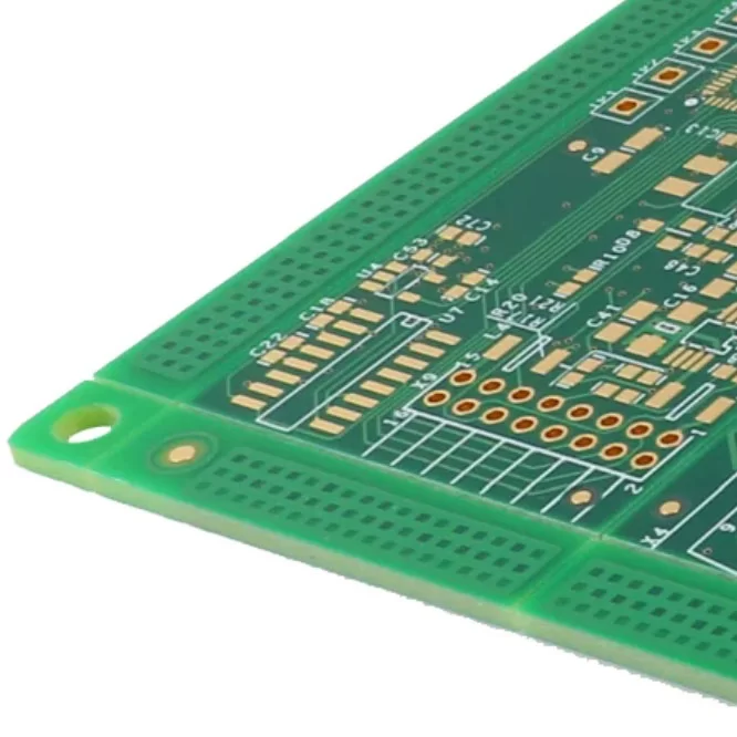
Printed Circuit Boards (PCBs) are an essential part of almost every modern electronic device. From simple hobby projects and educational kits to industrial controllers, home appliances, automotive systems, and advanced control equipment, PCBs provide a stable platform for connecting and operating electronic components.
During the early development of an electronic project, a breadboard is often used to test circuit concepts because components can be connected and changed quickly. However, as the circuit becomes more complicated, the large number of jumper wires can make the prototype difficult to organize, troubleshoot, and reproduce.
Once the circuit has been verified, transferring the design to a PCB creates a more compact and permanent solution. Understanding how to use PCB boards in electronic projects involves more than simply mounting components on a board. It includes circuit design, PCB layout, board selection, fabrication, component assembly, and final testing.

Preparing the PCB for the Electronics
Before components can be installed, the PCB needs to be designed according to the electrical requirements of the project. A well-prepared board can simplify assembly, improve circuit performance, and reduce potential problems during testing.
Design the Circuit:
The first stage is to create a schematic that represents the electrical relationships between all components. The schematic should include power sources, resistors, capacitors, ICs, connectors, sensors, and other required devices.
ECAD software such as KiCad, EasyEDA, and Altium Designer can be used to draw the schematic and check electrical relationships. Depending on the software and project, simulation and electrical rule checking can also be performed before moving to PCB layout.
Plan the Layout:
After the schematic has been verified, it is converted into a physical board layout. Component placement and routing should be planned according to electrical, mechanical, and thermal requirements.
Important layout considerations include:
Position related components close to one another when appropriate to shorten signal paths.
Place frequently used connectors and interfaces where they can be accessed easily after installation.
Use suitable trace widths based on current requirements rather than applying the same width to every connection.
Provide an appropriate ground plane for circuits that benefit from improved grounding and reduced interference.
Keep sensitive signal traces away from noisy or high-current sections when necessary.
Allow enough clearance around power components, regulators, and other heat-generating devices.
Provide suitable locations for heat sinks or other thermal management structures when required.
A carefully planned layout can make assembly and inspection easier while also helping the completed circuit achieve stable electrical performance.
Select the PCB Type:
PCB selection should be based on the electrical, mechanical, environmental, and manufacturing requirements of the project.
A simple circuit may work well with a single-layer or double-layer rigid PCB, while more complicated designs can benefit from multilayer construction. Flexible PCBs are suitable for applications where the circuit must bend or fit into a limited space, while rigid-flex boards combine rigid and flexible sections.
Material selection is also important. Standard FR-4 is widely used for general electronic applications, while specialized materials or metal-core PCBs may be selected when thermal performance, high-frequency behavior, flexibility, or other specific requirements become important.
PCB Fabrication:
After the schematic, layout, and board specifications have been finalized, manufacturing files can be generated for PCB fabrication. Gerber files are commonly used to communicate the required board layers and manufacturing information to the PCB manufacturer.
The fabrication process may include circuit imaging, copper processing, drilling, lamination for multilayer boards, surface finishing, solder mask application, and electrical inspection. For simple prototypes, some hobbyists may also use home PCB fabrication techniques, although professional manufacturing generally provides greater consistency and production reliability.

Steps to Use PCB in Your Projects
After the PCB has been manufactured, the next stage is to populate the board with its electronic components and verify that the assembled circuit performs as intended.
The exact assembly process depends on the board design and production method, but the following steps provide a practical workflow for many prototype and small-scale electronic projects.
1. Gather the Components:
Start by preparing every component required for the assembly. Most ECAD programs can generate a Bill of Materials (BOM), which provides information such as component references, values, package types, and quantities.
Review the BOM carefully before assembly to ensure that the required parts are available and that components with similar appearances or values are not accidentally mixed. Proper component preparation can significantly reduce assembly mistakes.
2. Place the Components on the PCB:
Once the components are ready, install them according to the PCB assembly drawing or component reference designators.
For hand assembly, it is often convenient to begin with smaller and lower-profile components before installing larger components and connectors. Check component values and orientation during placement, especially for polarized devices such as diodes, LEDs, electrolytic capacitors, and certain IC packages.
Correct placement at this stage helps prevent problems that can otherwise become difficult to diagnose after soldering.
3. Solder the Components:
Soldering creates both the mechanical attachment and electrical connection between the components and PCB pads.
For manual assembly, use an appropriate soldering iron, suitable solder, and proper temperature settings. Each joint should provide a secure connection without excessive solder or unintended bridges between adjacent pads.
Pay particular attention to fine-pitch ICs and densely populated areas because a small solder bridge can create a short circuit and affect the entire circuit.
4. Test and Inspect the Board:
After assembly, inspect the PCB carefully before applying power. Check component orientation, solder joints, connectors, and the board surface for visible defects.
A multimeter can be used to check continuity and identify potential short circuits, particularly between power and ground. Compare the assembled board with the schematic and layout files to confirm that all major components are installed correctly.
If the preliminary inspection is successful, apply power under controlled conditions and measure important voltage points. The circuit can then be tested according to its intended functions and operating requirements.
Once the board passes inspection and functional testing, it can be integrated into the larger electronic project.
Conclusion
Using a PCB can turn a tested circuit concept into a compact, repeatable, and practical electronic assembly. The process starts with creating and verifying the schematic, followed by component placement, PCB routing, board selection, fabrication, assembly, and testing.
Understanding how to use PCB boards in electronic projects also means considering electrical performance, component compatibility, thermal requirements, manufacturing limitations, and testing procedures throughout the development process.
For beginners, a simple PCB project can provide valuable experience with circuit design and electronic assembly. As project requirements become more advanced, the same workflow can be expanded to include multilayer boards, high-speed routing, flexible circuits, thermal management, automated assembly, and professional testing.
With careful planning and systematic testing, PCB-based projects can become more reliable, easier to reproduce, and better suited for practical electronic applications.