The continuous development of electronics has driven manufacturers toward smaller components, higher circuit density, and more compact product designs. Devices that once required large enclosures can now deliver significantly more functions in much smaller spaces. This progress has placed greater demands on PCB design, component selection, manufacturing precision, and assembly processes.
PCB assembly has changed considerably alongside this trend. Traditional through-hole components remain useful in applications that require mechanical strength, while surface mount devices have become widely adopted for compact and high-density electronic products. As component packages become smaller and placement tolerances become tighter, PCB assembly requires increasingly precise equipment and process control.
Understanding how to assemble PCB boards is therefore important for achieving consistent solder joints, accurate component placement, reliable electrical connections, and stable product performance.

What is PCB Assembly?
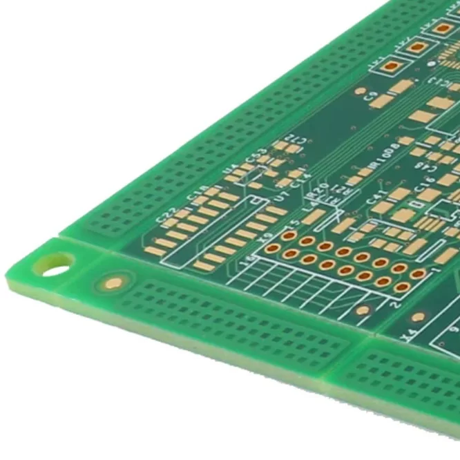
PCB assembly, commonly referred to as PCBA, is the manufacturing process of attaching electronic components to a fabricated bare PCB. Depending on the product design, components may be mounted using surface mount technology, through-hole technology, or a combination of both.
The process generally includes component preparation, solder paste application or other soldering preparation, component placement, soldering, inspection, and functional or electrical testing. PCB assembly begins after bare-board fabrication and transforms the unpopulated PCB into a functional electronic assembly.
Different products require different assembly approaches. The three major PCB assembly types include the following:
· Through-Hole PCB Assembly. Through-hole assembly uses components with leads that pass through drilled holes in the PCB. The leads are inserted into the board and soldered to the corresponding pads, commonly through wave soldering or selective soldering processes. This approach provides strong mechanical connections and continues to be useful for connectors, power components, and applications exposed to mechanical stress.
· Surface Mount Technology PCB Assembly. Surface Mount Technology (SMT) places components directly onto copper pads on the PCB surface rather than passing leads through drilled holes. Solder paste is deposited onto the pads before components are accurately positioned and soldered in a reflow oven. SMT allows manufacturers to use smaller packages and achieve higher component density, making it an important method for modern electronics production.
· Mixed PCB Assembly. Many electronic products contain both surface mount and through-hole components. In these cases, manufacturers use mixed-technology assembly to accommodate different component requirements. SMT components may be processed through reflow soldering, while through-hole components can be soldered using wave or selective soldering depending on the board design.
How to Assemble PCB Boards?
Modern SMT production relies on automated equipment and carefully controlled process parameters. Each stage affects the quality of the following operation, so the process must be properly coordinated from solder paste printing through final inspection.
· Solder Paste Printing: The assembly process normally begins with applying solder paste to the designated PCB pads. A metal stencil is positioned over the board, and a squeegee moves the paste across the stencil so that the material passes through precisely designed apertures. The amount and distribution of solder paste must be controlled to provide a suitable foundation for subsequent component soldering.
· Solder Pick and Place: Once the solder paste has been deposited, automated Pick-and-Place equipment positions components onto their corresponding pads. The machine uses programmed coordinates, component libraries, feeders, and vision systems to control component orientation and placement accuracy. Proper feeder setup and machine calibration are important for maintaining consistent placement throughout production.
· Reflow Soldering: After component placement, the assembled PCB passes through a reflow oven. The board is exposed to controlled temperature zones that gradually heat the solder paste, activate the flux, melt the solder alloy, and form permanent solder joints as the board cools. The thermal profile must be matched to the solder paste and component requirements to avoid overheating or insufficient soldering.
· Post Reflow Inspection: After reflow, the PCB is inspected to identify soldering and placement defects. Automated Optical Inspection (AOI) can check component position, polarity, solder coverage, and visible solder joints. For packages with hidden connections, such as certain BGAs, X-ray inspection can provide additional information about solder joint formation, voids, and other internal defects.
What are the Guidelines to Assemble PCB Boards Correctly?
Consistent PCB assembly depends on controlling materials, equipment, process parameters, and inspection standards. Manufacturers should evaluate each stage before production begins and establish appropriate process windows for the specific PCB design.
· Understand Equipment Capabilities. Before production, verify that the Pick-and-Place machine can handle the component sizes, package types, placement accuracy, board dimensions, and component heights required by the design. Equipment limitations should be considered during both PCB design and manufacturing planning.
· Choose the Right Solder Paste Type. Solder paste selection should consider the PCB finish, component package, reflow process, environmental requirements, and applicable manufacturing standards. Factors such as alloy composition, flux characteristics, and powder particle size can influence printing quality and solder joint formation.
· Optimise Stencil Design. The stencil determines how much solder paste reaches each PCB pad. Aperture dimensions, stencil thickness, shape, and reduction ratios should be selected according to component geometry and pad design. Fine-pitch components may require more precise aperture engineering to prevent insufficient solder or excessive paste deposition.
· Fine-tune Reflow Process. Reflow temperature and time have a direct impact on solder joint quality. The thermal profile should follow the solder paste manufacturer's recommended process window while also considering component temperature limitations and PCB characteristics. Temperature measurements across representative board locations can help verify that the selected profile provides sufficient heating without creating excessive thermal stress.

What are the Common Issues Encountered during PCB Assembly?
PCB assembly defects can originate from material selection, stencil printing, component placement, reflow conditions, equipment settings, or PCB design. Identifying these problems early helps manufacturers prevent recurring defects and maintain consistent production quality.
· Solder Bridging. Solder bridging occurs when molten solder connects two or more adjacent pads or leads that should remain electrically isolated. It is more common in fine-pitch assemblies when solder paste volume, stencil apertures, pad geometry, or placement accuracy is not properly controlled. Optimising the printing process and maintaining suitable stencil conditions can significantly reduce this defect.
· Missing and Misaligned Components. Components may be absent, incorrectly oriented, or positioned outside the required placement tolerance. These problems can result from incorrect feeder setup, component recognition errors, programming mistakes, or machine calibration issues. Vision systems, accurate component libraries, and appropriate machine verification procedures help reduce placement-related defects.
· Tombstoning. Tombstoning occurs when one end of a small passive component rises from the PCB pad during reflow, leaving the component standing at an angle. Uneven solder paste deposition, differences in pad heating, pad design, or unbalanced soldering forces can contribute to this problem. Consistent paste printing and a properly tuned reflow profile are important for controlling tombstoning.
· Solder Balls. Solder balls are small particles of solder that remain outside the intended solder joints. They may be associated with excessive solder paste, unsuitable reflow conditions, moisture, contamination, or stencil-printing problems. Maintaining clean production equipment, controlling paste volume, and following appropriate storage and handling procedures can help minimize their occurrence.
Conclusion
Reliable PCB assembly depends on much more than placing components onto a circuit board. Every stage, from solder paste printing and component placement to reflow and inspection, needs to be controlled according to the board design and component requirements. A well-defined process helps manufacturers achieve consistent solder joints, accurate placement, and dependable electrical performance.
Understanding how to assemble PCB boards also helps engineers and manufacturers identify potential production risks before they become large-scale manufacturing problems. Proper equipment selection, stencil optimisation, solder paste management, thermal profiling, and automated inspection all contribute to a stable assembly process.