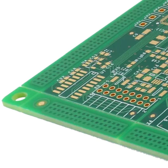
Choosing the right prototyping board is an important step in developing and testing electronic circuits. Zero PCB and General Purpose PCB are both widely used for building experimental circuits, but their copper layouts, wiring methods, and practical uses may vary. Understanding the difference between Zero PCB and General Purpose PCB helps students, hobbyists, and engineers select a suitable board for their projects. This guide explains their characteristics, advantages, limitations, and common applications to help you make an informed decision.

What is a Zero PCB?
A Zero PCB is a prototyping board designed with a grid of holes, typically spaced 2.54 mm (0.1 inch) apart. Each hole is surrounded by an individual copper pad that remains electrically isolated from neighboring pads. Because the board does not contain predefined circuit traces, users must create electrical connections themselves using solder bridges, jumper wires, or other suitable wiring methods.
This open layout provides considerable freedom when arranging components and building custom circuits. Designers can determine the connection paths according to their schematic rather than adapting their circuits to an existing copper pattern. A Zero PCB is therefore useful for experimental electronics, small hardware projects, and early-stage circuit development.
The name generally refers to a board without preset conductive tracks connecting its component pads. However, product specifications can differ among suppliers, so it is advisable to confirm the actual copper pattern before purchasing.
What is a General Purpose PCB?
A General Purpose PCB, also called a General Purpose Printed Circuit Board (GP PCB), is a versatile board intended for assembling, evaluating, and modifying electronic circuits before moving to a custom-manufactured PCB. Many versions feature a standard 2.54 mm (0.1-inch) hole grid, making them suitable for numerous through-hole components, including resistors, capacitors, connectors, and DIP integrated circuits.
Unlike a strictly isolated-pad layout, the term General Purpose PCB can describe several types of universal prototyping boards. Some models have individually isolated copper pads, while others feature connected copper strips or alternative conductive patterns. These differences affect how components must be wired and how easily the circuit can be modified.
Before selecting a General Purpose PCB, check its pad arrangement, board dimensions, substrate material, and compatibility with the intended components. Choosing a layout that matches the project can reduce wiring effort and simplify assembly.
Zero PCB vs General Purpose PCB: Key Differences
Zero PCB and General Purpose PCB both support hands-on circuit development without requiring a custom PCB for every design change. Their practical differences depend largely on the board's copper pattern and physical construction. In particular, understanding whether the pads are isolated or connected is essential when planning the circuit layout.
Design Flexibility: Zero PCB typically provides isolated copper pads, allowing users to create their own connections. General Purpose PCBs may offer the same arrangement or include connected copper patterns, which can influence wiring options.
Assembly: Both board types generally require manual component installation and soldering. The amount of jumper wiring and the complexity of the assembly depend on the selected layout.
Modification: Circuits on isolated-pad boards can often be adjusted by removing or adding wires and solder connections. Changes to boards with connected copper strips may require additional cutting or isolation work.
Durability: Soldered prototype boards can provide more stable mechanical and electrical connections than temporary, unsoldered breadboard assemblies. Actual durability depends on solder quality, component support, materials, and operating conditions.
Applications: Both options are suitable for DIY electronics, educational experiments, robotics, circuit testing, and early-stage product development.
Comparison Table: Zero PCB vs General Purpose PCB
Comparison Point | Zero PCB | General Purpose PCB |
Definition | A prototyping board typically featuring isolated copper pads without predefined connecting traces. | A versatile circuit prototyping board that may use isolated pads or other universal copper patterns. |
Copper Pattern | Usually consists of individual, electrically isolated copper pads. | Varies by manufacturer and model; may feature isolated pads, connected strips, or other layouts. |
Hole Spacing | Commonly 2.54 mm (0.1 inch). | Often 2.54 mm (0.1 inch), depending on the product design. |
Circuit Flexibility | Supports customized wiring because users establish the electrical connections. | Suitable for flexible prototyping, with wiring options determined by the copper arrangement. |
Assembly | Components are soldered manually, with jumpers or solder bridges used to form connections. | Typically assembled by hand, with the process depending on the board's conductive pattern. |
Modification | Circuit changes can be made by reworking solder joints and wiring. | Revisions are possible, although connected copper patterns may require extra work. |
Durability | Soldered connections can support practical prototype use when assembled correctly. | Offers similar potential durability when the materials and solder joints are appropriate. |
Cost | Generally an economical option for experimental circuits. | Usually affordable and available in a range of sizes and configurations. |
Best Use | Custom wiring, Arduino projects, robotics, DIY electronics, and circuit experiments. | General electronics prototyping, education, repair tasks, and laboratory development. |
Typical Users | Students, hobbyists, engineers, and hardware developers. | Students, technicians, hobbyists, and electronics engineers. |
Production Suitability | Primarily intended for prototyping rather than commercial mass production. | Generally used for prototypes and experiments rather than production-scale manufacturing. |
Features of Zero PCB
Standard Hole Spacing: Many Zero PCBs use a 2.54 mm (0.1-inch) grid, making it convenient to install a wide range of through-hole components.
Isolated Copper Pads: Each pad provides a separate soldering point, allowing users to determine which components are electrically connected.
Unrestricted Connection Layout: Without predefined copper traces, designers can build customized circuits using jumper wires and soldered connections.
Multiple Substrate Options: Depending on the supplier, Zero PCBs may be available in FR2 or FR4 materials to suit different project requirements.
Single-Sided and Double-Sided Designs: Some models provide copper pads on one side, while others offer conductive pads on both sides for more flexible assembly.
Features of General Purpose PCB
Versatile Circuit Development: General Purpose PCBs support the assembly and evaluation of different electronic circuits before a dedicated board is manufactured.
Compatibility with Common Components: Many models use 2.54 mm (0.1-inch) spacing, accommodating through-hole resistors, capacitors, connectors, and DIP ICs.
Different Board Sizes: A variety of dimensions allows users to select a board that fits the circuit's component count and physical layout.
Available Substrate Materials: FR2 and FR4 options may be offered, with the appropriate choice depending on mechanical strength, thermal demands, and budget.
Convenient Design Adjustments: Components and wiring can be rearranged during development, subject to the board's copper pattern and available space.
Advantages and Disadvantages of Zero PCB
Advantages:
Flexible Circuit Arrangement: Isolated pads give users control over connection paths, making the board suitable for circuits with customized wiring requirements.
Low-Cost Experimentation: A Zero PCB provides an affordable way to evaluate circuit concepts without immediately ordering a custom-manufactured board.
Practical Learning Experience: Building circuits by hand helps users develop soldering skills and understand component connections and circuit behavior.
Disadvantages:
Labor-Intensive Assembly: Each connection must be created manually, which can increase assembly time as the circuit becomes larger.
More Difficult Troubleshooting: Dense wiring and numerous solder joints can make fault detection, maintenance, and circuit tracing more challenging.
Limited Production Use: Hand-assembled prototype boards may not deliver the repeatability, compactness, or manufacturing consistency required for commercial products.
Advantages and Disadvantages of General Purpose PCB
Advantages:
Broad Application Range: General Purpose PCBs can support a variety of educational, experimental, repair, and engineering projects.
Suitable for Iterative Development: Their accessible layout makes it possible to test circuit ideas and make changes before committing to a custom PCB design.
Economical and Accessible: These boards are commonly used for small-scale projects because they are relatively inexpensive and available in different configurations.
Disadvantages:
Manual Assembly Requirements: Component placement, soldering, and wiring usually require hands-on work, particularly when the board lacks connected copper patterns.
Challenges with Complex Circuits: A large number of components and connections can create crowded layouts, making assembly and debugging more difficult.
Not a Replacement for Production PCBs: General-purpose prototype boards are not normally designed to meet the space, consistency, and manufacturing requirements of finished electronic products.
Applications of Zero PCB
Zero PCB is commonly used when developers need to assemble a circuit quickly without designing and manufacturing a dedicated board. Its isolated copper pads allow users to establish custom connections, making it suitable for educational exercises, hardware experiments, and early-stage product testing.
Arduino Projects
Zero PCBs can be used to build custom Arduino expansion boards, sensor interfaces, relay circuits, and motor-control prototypes. Developers can connect external components to the required pins and test how different modules interact with the microcontroller before designing a compact, dedicated PCB.
Raspberry Pi Add-ons
For Raspberry Pi projects, Zero PCBs offer a practical way to assemble GPIO interfaces, sensor circuits, relay modules, and other hardware accessories. They allow hobbyists to explore circuit connections and validate peripheral functions without waiting for a custom board to be fabricated.
DIY Electronics
DIY enthusiasts can use Zero PCBs to construct small electronic devices such as LED controllers, audio amplifiers, simple automation circuits, and experimental power-control systems. The ability to choose individual connection paths makes the board useful for learning and adapting circuit designs to specific project needs.
Robotics
Robotics projects often combine motors, sensors, communication modules, and power-distribution circuits. A Zero PCB can serve as a platform for connecting these elements during development, helping builders test signal paths and hardware interactions before moving to a more integrated circuit board.
STEM Education
Schools, colleges, and electronics training laboratories can use Zero PCBs to introduce students to soldering, circuit assembly, and basic electronic principles. By constructing working circuits, learners can observe how components are connected and gain practical experience in identifying and correcting wiring errors.
Prototype Development
Engineers may use Zero PCBs to verify circuit functionality, evaluate component arrangements, and test preliminary hardware concepts. This approach is particularly useful when a design is still changing and a custom PCB would be premature. Once the circuit has been validated, the design can be transferred to a purpose-built board.
Circuit Repair
A Zero PCB can help technicians assemble temporary test circuits, replace unavailable board sections in experimental equipment, or evaluate alternative component connections. For permanent repairs, the technician should still consider electrical ratings, mechanical stability, insulation, and the safety requirements of the equipment.
Applications of General Purpose PCB
General Purpose PCBs provide a convenient platform for building and modifying circuits during development. Their different pad and copper configurations make them useful across education, electronics maintenance, laboratory experiments, and preliminary hardware evaluation.
Electronics Prototyping
Engineers can use General Purpose PCBs to assemble circuit concepts and check whether components work together as expected. They can test signal connections, verify basic functions, and make adjustments before committing to the layout and fabrication costs of a custom PCB.
Circuit Repair and Maintenance
Technicians may use a General Purpose PCB to build replacement circuit sections, test alternative wiring arrangements, or modify noncritical hardware when a dedicated board is unavailable. The selected board must match the circuit's electrical and mechanical requirements, particularly when handling higher currents or elevated temperatures.
Educational Projects
General Purpose PCBs are useful in classrooms and training workshops where students learn about component placement, soldering, circuit continuity, and basic troubleshooting. Instructors can use them for practical exercises that demonstrate how schematic diagrams translate into physical electronic circuits.
DIY Electronics
Hobbyists can assemble projects such as timer circuits, LED drivers, audio amplifiers, small power supplies, and home-automation prototypes on a General Purpose PCB. The board provides a solderable alternative to temporary breadboard setups when a project requires more stable connections.
Product Development
During early product development, engineers can use a General Purpose PCB to evaluate hardware functionality and explore component arrangements. It offers a practical intermediate step between initial circuit experiments and the development of a professionally designed PCB, especially when the design still requires refinement.
Laboratory Testing
Research laboratories and electronics development teams can use General Purpose PCBs to build test fixtures, connect experimental components, and investigate circuit behavior. A suitable board can simplify short-term experiments and make it easier to replace components or revise connections as testing progresses.

Zero PCB vs General Purpose PCB: Which One Should You Choose?
The choice between Zero PCB and General Purpose PCB depends on the circuit's complexity, wiring preferences, available space, and development objectives. Because the two terms can overlap in the market, checking the actual copper layout is often more useful than relying on the product name alone.
Students and Beginners: A Zero PCB with isolated pads can be a good starting point for learning soldering and understanding how electronic components connect. Beginners should select a board size that provides enough space to work safely and clearly.
DIY Electronics Projects: Either board can work well for small circuits such as LED controllers, timers, audio projects, and basic automation devices. The best option depends on whether isolated pads or a predefined copper pattern better suits the design.
Arduino and Raspberry Pi Projects: Both board types can be used to prototype sensor interfaces, expansion circuits, communication modules, and motor-control hardware. Confirm the pin spacing, connection layout, and power requirements before assembly.
Engineers and Product Developers: These boards support preliminary circuit validation, component testing, and hardware troubleshooting. For more complex designs, careful wiring documentation and testing are important before transferring the circuit to a custom PCB.
Production-Ready Products: Once the prototype has been verified, a custom-designed and professionally manufactured PCB is generally the better choice for repeatable assembly, optimized board space, and consistent product quality.
After confirming the circuit's functionality, the next step is to prepare a dedicated PCB design that meets the requirements of the intended application.
Common Mistakes When Choosing a Prototype PCB
Selecting a suitable prototype PCB can make circuit development more efficient and reduce unnecessary rework. The following mistakes are worth avoiding when comparing board options.
Choosing Without Checking the Copper Layout: Assuming every General Purpose PCB has the same pad arrangement can lead to unexpected wiring work. Review the actual copper pattern and determine whether it suits the circuit before purchasing.
Using a Breadboard for Long-Term Applications: Breadboards are convenient for temporary, solderless experiments, but their contacts may loosen under vibration or repeated handling. Soldered prototype boards can provide more stable connections, although they are not automatically suitable for every permanent application.
Using a Prototype Board for Mass Production: Prototype boards are useful for testing and experimentation, but they are generally not optimized for large-scale manufacturing. Once the design is stable, a professionally fabricated PCB offers better opportunities for repeatability, compact layouts, and controlled assembly.
Overlooking the Board Material: FR2 and FR4 boards differ in material properties, cost, and suitability for particular operating conditions. FR4 is commonly selected when better thermal and mechanical performance is required, but the final choice should reflect the project's specifications.
Selecting an Inappropriate Board Size: A board that is too small can make component placement, soldering, and troubleshooting difficult. An unnecessarily large board may increase material use and leave the circuit poorly organized. Allow enough room for wiring, clearances, and future adjustments.
Conclusion
Zero PCB and General Purpose PCB are both practical options for building, testing, and refining electronic circuits before investing in custom PCB fabrication. Zero PCB typically emphasizes isolated copper pads and user-defined wiring, while General Purpose PCB is a broader category that may include several different copper layouts. Understanding these distinctions, along with the advantages, limitations, and typical applications of each board, can help you choose the right platform for your project.
For designs intended for commercial use, a prototype board should be viewed as a development tool rather than the final manufacturing solution. Once the circuit has been tested and validated, moving to a professionally designed PCB can improve layout efficiency, assembly consistency, and suitability for production.
Ready to turn your prototype into a production-ready PCB?