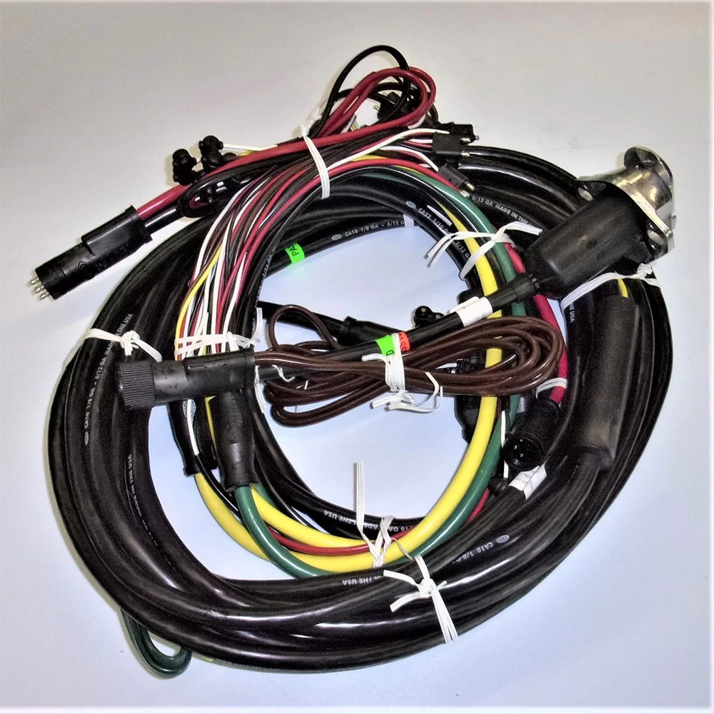
Wire soldering is an essential skill in electronics development, circuit board repair, and electronic product manufacturing. A properly soldered connection helps maintain stable electrical performance while preventing wires from loosening during handling, installation, or equipment operation.
Learning how to solder wire to PCB board correctly involves more than simply melting solder onto a copper pad. Wire selection, surface preparation, temperature control, solder application, and mechanical support all contribute to connection quality. This guide explains the complete process, including the tools you need, the steps for producing dependable solder joints, common mistakes to avoid, and methods for checking the finished connection.

What is PCB Wire Soldering?
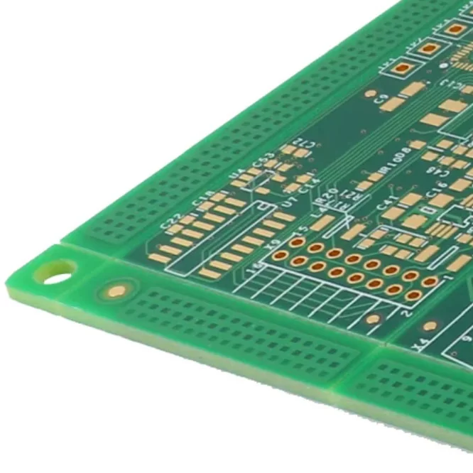
PCB wire soldering involves attaching an electrical conductor to a designated connection point on a printed circuit board using a suitable solder alloy. Depending on the board design, the wire may be connected through a plated hole, a dedicated terminal, or a copper surface pad.
During the process, the solder melts and bonds to the prepared conductive surfaces, establishing an electrical path between the wire and the circuit. A correctly formed joint should provide consistent conductivity without compromising the surrounding copper traces or electronic components.
This technique is widely used in prototype development, cable connections, power supply circuits, sensor interfaces, and electronic equipment maintenance. Poorly formed joints can introduce electrical resistance, cause intermittent operation, or disconnect completely under mechanical stress.
Why Wire Soldering Is Important
Wires behave differently from rigid component leads because they can bend, twist, and move during normal use. These movements place additional stress on the point where a wire meets a PCB, particularly when the cable is repeatedly handled or exposed to vibration.
Reliable soldering helps maintain signal transmission, power delivery, and overall circuit stability. It also reduces the likelihood of loose connections, localized heating, and unexpected equipment failures.
For commercial electronics, the quality of each wire connection can influence product durability, assembly consistency, and maintenance requirements. Appropriate soldering techniques, combined with suitable strain relief, help protect the connection throughout the product's service life.
Through Hole vs Surface Wire Soldering
The appropriate connection method depends on the PCB layout, available mounting space, wire dimensions, and mechanical requirements.
Through-hole soldering involves inserting the stripped wire into a plated hole before applying solder. When the hole and pad are designed for the intended wire, this arrangement can provide a larger bonding area and better mechanical retention.
Surface soldering attaches the wire directly to an exposed copper pad without passing it through the board. This approach is useful for compact electronics, existing circuit board repairs, and designs where dedicated wire holes are unavailable.
Neither method is automatically suitable for every application. High-current connections, heavy cables, and products exposed to vibration may require dedicated terminals, connectors, or additional mechanical anchoring rather than relying on a solder joint alone.
Types of Wires Used for PCB Soldering
Wire construction influences flexibility, solderability, and resistance to repeated bending. Selecting a suitable conductor before starting the soldering process helps prevent installation difficulties and premature connection failures.
Wire Type | Best Use | Advantages | Limitations |
Solid Wire | Fixed connections and breadboard circuits | Maintains its shape and is easy to position | Can fatigue and fracture after repeated bending |
Stranded Wire | Flexible cables and moving assemblies | Offers good flexibility and resistance to bending fatigue | Loose strands must be controlled during soldering |
Tinned Copper Wire | Electronics requiring improved solderability and corrosion resistance | Tin coating helps reduce copper oxidation and supports solder wetting | May cost more than comparable untreated wire |
Solid Core Wire: Solid wire contains a single conductive core. Its rigidity makes it convenient for fixed circuit connections where the conductor will remain relatively stationary. It is less suitable for applications involving continuous movement.
Stranded Wire: Stranded wire consists of multiple fine copper filaments bundled together. Its flexibility makes it a common choice for electronic cables, portable devices, and assemblies where limited movement is expected. Twisting and lightly tinning the exposed strands helps prevent individual filaments from spreading during soldering.
Tinned Copper Wire: Tinned copper wire has a thin tin coating over its copper conductor. The coating improves solderability and helps protect the underlying copper from oxidation. It can be particularly useful in assemblies where storage conditions, humidity, or long-term connection reliability are important considerations.
Choosing the Correct Wire Gauge
Wire gauge affects current capacity, voltage drop, heat generation, and the physical fit of a connection. A conductor that is too thin may overheat under load, while an unnecessarily thick wire can be difficult to position on a small PCB pad.
The following ranges provide a general starting point for low-voltage electronic applications. Final selection should account for current, conductor length, insulation temperature rating, ambient conditions, and applicable electrical standards.
Application | Recommended Wire Gauge |
Signal wires | 26–30 AWG |
Sensors | 24–28 AWG |
Low-power circuits | 22–24 AWG |
Power distribution | 18–22 AWG |
High-current connections | 14–18 AWG |
These ranges are not universal design limits. High-current wiring may require a larger conductor, and the PCB pad, terminal, and copper trace must also be rated for the intended load. Always verify the actual electrical requirements before selecting a wire size.
Tools Required for Soldering Wire to PCB
Preparing the necessary tools before beginning makes the process more controlled and reduces the risk of damaging the board. Consistent heat delivery, accurate wire preparation, and reliable inspection are particularly important when working with small pads or sensitive electronic components.
Soldering Iron: A temperature-controlled soldering iron rated around 40–70 W is suitable for many general PCB soldering tasks. Adjustable temperature settings help accommodate different solder alloys, pad sizes, and wire thicknesses. The correct tip and heat transfer are more important than wattage alone.
Solder Wire: Electronic-grade solder wire is commonly available in diameters from approximately 0.6 mm to 1.0 mm. Fine solder wire provides better control on small pads, while a larger diameter can be convenient for larger terminals and conductors.
Flux: Flux removes or disrupts surface oxides and helps molten solder wet the metal surfaces. Although many electronic solder wires contain flux, a compatible additional flux can improve results when the pad or conductor is difficult to solder.
Wire Preparation Tools: Wire strippers, precision cutters, tweezers, and PCB holders simplify the preparation process. Proper stripping prevents conductor damage, while a stable fixture keeps the wire and circuit board correctly positioned.
Inspection Equipment: A magnifier, suitable lighting, and a digital multimeter help identify incomplete solder joints, unintended connections, and open circuits. For sensitive or high-reliability assemblies, additional inspection methods may be necessary.
Choosing the Right Solder and Flux
Solder alloy and flux chemistry affect melting temperature, wetting behavior, residue, and the final connection's suitability for its operating environment. Selecting compatible materials helps produce repeatable results and avoids unnecessary stress on the PCB.
Leaded Solder
Traditional tin-lead alloys, such as Sn60Pb40, have a relatively low melting temperature and generally offer predictable wetting behavior. They remain useful for certain repair and development tasks where their use is permitted.
Because lead presents health and environmental risks, leaded solder should be handled with appropriate hygiene and ventilation practices. Its use may also be restricted by product requirements and regulations.
Lead Free Solder
Lead-free alloys are widely used in commercial electronics manufacturing to meet applicable environmental requirements. Common SAC alloys contain tin, silver, and copper. Their melting temperatures and working characteristics differ from those of conventional tin-lead solder, so temperature settings and process parameters may need adjustment.
Lead-free solder is not automatically compliant with every regulation or product specification. The selected alloy must match the assembly requirements and applicable standards.
Rosin Flux
Rosin-based flux is commonly used for manual electronics soldering because it assists wetting and helps remove surface oxides during heating. Different formulations leave different amounts of residue, so the manufacturer's recommendations should determine whether cleaning is necessary.
No-Clean and Water-Soluble Flux
No-clean flux is designed to leave residues that may not require removal under specified conditions. However, its suitability depends on the flux formulation, electrical requirements, and operating environment.
Water-soluble flux offers effective cleaning action but generally requires thorough removal according to the manufacturer's instructions. Residues left behind can affect reliability, especially in moisture-sensitive applications.
Choosing the Right Soldering Iron Tip
The soldering tip should match the dimensions of the wire and the copper pad. A suitable tip transfers heat efficiently, allowing the joint to reach working temperature without unnecessarily prolonged contact.
Conical tips provide access to confined areas and small connection points. Chisel tips offer a broader contact surface and are often more effective for larger pads or thicker wires because they transfer heat efficiently.
A tip that is too small may struggle to heat the joint evenly, while an excessively large tip can interfere with adjacent components. Keep the tip clean, properly tinned, and compatible with the soldering station to maintain consistent performance.
Preparing the PCB and Wire
Careful preparation reduces soldering time and improves the likelihood of achieving a reliable electrical connection. Before applying heat, inspect the connection area, confirm that the wire is suitable for the pad, and make sure the workpiece is securely supported.
Clean the PCB Pads: Remove dust, grease, and other contaminants from the soldering area using an appropriate electronics-grade cleaning method. Isopropyl alcohol can be useful when compatible with the board and its components. If a pad is heavily oxidized or damaged, assess its condition before proceeding.
Strip the Wire Correctly: Remove approximately 3–5 mm of insulation when appropriate for the pad or through-hole dimensions. The exposed length should be sufficient for the connection without leaving unnecessary bare conductor. Avoid cutting or nicking the copper strands during stripping.
Twist and Tin the Wire: Gently twist stranded conductors to keep the filaments together, then apply a thin layer of solder if the connection method calls for pre-tinning. This makes positioning easier and helps prevent loose strands from touching neighboring pads. Avoid excessive solder buildup that could prevent the wire from fitting into its designated hole.
Apply Flux: Add a small amount of compatible electronics flux to the conductor and pad when needed. Flux supports wetting during heating, particularly when surface oxidation interferes with solder flow.
Secure the PCB: Place the circuit board in a stable holder and position the wire so that it remains in contact with the intended connection point. A secure setup reduces movement during soldering and makes it easier to control the iron accurately.
Step-by-Step Guide to Solder Wire to PCB
Following a consistent sequence makes it easier to control heat, solder quantity, and wire placement. The goal is to heat the conductor and pad sufficiently for the solder to wet both surfaces, without exposing the PCB to excessive thermal stress.
Position the Wire: Insert the prepared conductor into the designated plated hole or place it against the intended surface pad. Check that the exposed copper does not overlap adjacent conductive areas and that the wire remains stable throughout the process.
Heat Wire and Pad: Place the soldering iron tip so that it contacts both the wire and the pad when the geometry allows. This helps bring both surfaces to a suitable temperature. The required heating time depends on the tip, pad size, wire thickness, and solder alloy; avoid treating a fixed number of seconds as a universal rule.
Feed the Solder: Apply solder to the heated joint rather than relying on the iron tip alone to melt a large quantity of solder. When the surfaces reach the correct temperature, solder should flow across the conductor and pad, forming a continuous bond. Stop feeding once sufficient solder has covered the connection without obscuring its shape.
Remove the Heat: Withdraw the solder wire and then remove the soldering iron. Avoid dragging the tip across nearby pads or components. If the solder does not flow properly, stop and investigate the temperature, cleanliness, and flux rather than repeatedly heating the board.
Allow the Joint to Cool: Keep the wire still while the solder solidifies. Do not bend, pull, or reposition the conductor during cooling. Once the joint has stabilized, inspect it before applying any additional mechanical support.

How to Create a Strong Solder Joint
A dependable solder joint requires proper wetting, suitable solder volume, and adequate mechanical support. A large quantity of solder does not necessarily produce a stronger connection; the quality of the bond between the metal surfaces is more important.
Ensure Proper Heat Transfer: Both the wire and the PCB pad need to reach an appropriate soldering temperature. If the solder melts on the iron but fails to spread across the joint, the underlying surfaces may not be hot enough or may be contaminated.
Use the Right Amount of Solder: Apply enough solder to establish a continuous connection without creating excessive buildup. Too little solder may leave portions of the connection inadequately bonded, while too much can conceal defects or bridge adjacent pads.
Let the Solder Cool: Avoid disturbing the wire until the solder has solidified. Movement during this stage can disrupt the joint structure and produce cracks or an unreliable connection. Mechanical support should be added only after the joint has cooled and been inspected.
Good vs. Bad Solder Joints
Visual appearance provides useful clues about solder quality, although appearance alone cannot confirm electrical or mechanical reliability. Lead-free solder may have a less shiny finish than traditional leaded solder, so surface brightness should not be used as the only acceptance criterion.
Solder Joint | Appearance | Likely Cause | Recommended Fix |
Good Joint | Smooth, continuous wetting with a suitable fillet | Appropriate heating and solder application | Accept if it meets the design requirements |
Cold Joint | Uneven surface or incomplete wetting | Insufficient heat, contamination, or movement during cooling | Rework using suitable flux and controlled heating |
Solder Bridge | Unintended solder connection between neighboring conductors | Excess solder or poor placement | Remove the bridge and inspect for damage |
Insufficient Solder | Incomplete coverage or weak bonding | Inadequate solder application or poor wetting | Rework after checking surface condition |
Overheated Joint | Damaged pad, discolored laminate, or lifted copper | Excessive thermal exposure | Assess the board and repair or replace damaged areas |
Common Soldering Mistakes
Even when the basic soldering process seems straightforward, small errors can affect electrical performance and long-term durability. Recognizing these issues helps reduce rework and improves consistency across prototype and production assemblies.
Using Too Much Heat
Excessive temperature or prolonged contact can damage PCB laminate, lift copper pads, and affect nearby components. Use a suitable temperature setting, an appropriate tip, and controlled heating. If a joint does not form promptly, investigate the cause instead of continuing to apply heat.
Applying Excessive Solder
Large solder deposits can conceal incomplete wetting and increase the risk of short circuits between nearby pads. Apply solder gradually and stop when the conductor and pad have a continuous, adequately formed joint.
Skipping Flux
Oxidized metal surfaces can prevent solder from spreading evenly. Suitable flux helps remove surface oxides and improves wetting. If solder beads up instead of bonding to the metal, check surface cleanliness and flux compatibility before attempting another joint.
Using Dirty Soldering Tips
Oxidized tips transfer heat poorly and may contaminate the connection. Clean the tip with an appropriate brass cleaner or the soldering station manufacturer's recommended method, then maintain a thin protective layer of solder when the tip is not actively being used.
Choosing the Wrong Wire Size
A wire that is too thick may not fit the designated pad or hole and can place unnecessary stress on the copper connection. A wire that is too thin may not safely carry the intended current. Select the conductor according to electrical requirements, board geometry, and mechanical conditions.
Troubleshooting Common Problems
If solder refuses to spread, inspect the pad and wire for contamination, confirm that the iron is transferring heat effectively, and apply compatible flux where appropriate. For a joint with incomplete wetting, controlled rework may restore the connection.
When solder bridges adjacent pads, disconnect the power source and remove the excess solder with suitable desoldering braid or a desoldering tool. Inspect the surrounding copper for damage before testing the board again. If a pad has lifted or a trace has been damaged, additional solder alone will not provide a reliable repair.
How to Inspect Soldered Connections
Inspection helps identify defects before the PCB is integrated into a larger assembly or energized. A good inspection routine combines visual checks with appropriate electrical tests rather than relying on appearance alone.
Perform a Visual Inspection: Examine each connection under good lighting, using magnification where necessary. Look for incomplete wetting, cracks, solder bridges, excessive solder, damaged pads, and loose wire strands. The joint should match the acceptance criteria for the selected solder alloy and assembly process.
Check Mechanical Strength: After the joint has cooled, confirm that the wire is securely positioned. Avoid forceful pull tests that could damage the pad or trace. If the product requires a defined pull-force test, follow the applicable test procedure and specified limits.
Test for Electrical Conductivity: Use a digital multimeter to check continuity between the intended connection points. Disconnect power before performing resistance or continuity measurements unless the equipment specifically requires another approved test method. Remember that continuity alone does not establish that a joint can safely carry its rated current.
Look for Nearby Shorts: Inspect neighboring pads, exposed traces, and component terminals for unintended solder connections. A short circuit may cause malfunction or damage when power is applied, so verify isolation between conductors where the circuit design requires it.
Follow a Final Inspection Checklist: Before energizing the board, confirm that the joints are properly wetted, mechanically supported where necessary, and free from solder bridges or visible damage. Check continuity and isolation as appropriate, and remove flux residue when required by the selected material and assembly specifications.
Wire Strain Relief Techniques
Solder establishes the electrical connection, but it should not be expected to absorb continuous pulling, bending, or cable movement. Repeated mechanical stress can fatigue the conductor, crack the solder joint, or detach the copper pad from the PCB.
Strain relief transfers these loads to a more suitable support point, helping extend the service life of the assembly.
Heat Shrink Tubing
Heat shrink tubing insulates exposed conductors and can provide limited support around a wire connection when appropriately positioned. Its effectiveness depends on the tubing design, attachment method, and available anchoring area. It should not be treated as a substitute for proper cable anchoring in high-stress applications.
Hot Glue
Hot-melt adhesive can help hold lightweight wires in place in prototypes and low-stress electronic assemblies. Before applying it, verify that the adhesive's temperature resistance and compatibility are suitable for the PCB and surrounding components. It is generally not a universal solution for high-temperature or demanding industrial environments.
Epoxy Adhesive
A suitable two-part epoxy can secure wire insulation or a designated anchoring area to the board. Once cured, it can provide durable mechanical support. Choose a formulation compatible with the PCB materials, operating temperature, and expected stresses, and avoid covering components or areas that require future maintenance.
Cable Ties and Mounting Points
Where the enclosure or PCB assembly provides cable anchors, clips, or mounting holes, these features can support the cable independently of the solder joint. Proper anchoring is particularly important for heavy cables and equipment exposed to vibration.
Proper Cable Routing
Route wires with gradual bends and sufficient clearance from sharp edges, moving components, and hot surfaces. Leave enough slack for normal assembly tolerances without allowing the cable to pull on the soldered connection. Good cable routing reduces stress concentration and helps prevent conductor fatigue.
Safety Tips for PCB Soldering
PCB soldering involves hot tools, molten metal, flux emissions, and potentially hazardous materials. Appropriate precautions protect the operator, the circuit board, and the surrounding work area.
Work in a Well-Ventilated Area
Soldering can release fumes containing flux decomposition products. Use effective local exhaust ventilation or a suitable fume extractor to remove emissions from the breathing zone. General room ventilation alone may not provide adequate control for frequent soldering work.
Wear Appropriate Eye Protection
Safety glasses help protect against solder splashes, clipped wire fragments, and debris produced during trimming or rework. Eye protection is particularly important when cutting stranded wire or working with small components.
Handle the Soldering Iron Carefully
Soldering iron tips can reach temperatures above 350°C, depending on the setting. Always return the tool to its stable stand when not in use, keep the heated tip away from cables and flammable materials, and allow the equipment to cool before storage or maintenance.
Protect Sensitive Electronics from Static Charges
Use appropriate electrostatic discharge protection when handling static-sensitive components. An ESD-safe workstation and correctly grounded wrist strap can reduce the risk of damage from electrostatic discharge.
Maintain a Clean Workspace
Keep tools organized and remove loose wire fragments, solder debris, and other waste from the work surface. Store solder and flux according to their safety instructions, wash hands after handling soldering materials, and follow applicable procedures for lead-containing waste.
Conclusion
Learning how to solder wire to PCB board correctly helps improve electrical continuity, connection stability, and the overall reliability of electronic assemblies. Successful results depend on choosing the right wire gauge, using compatible solder and flux, preparing the metal surfaces, controlling heat, and allowing the finished joint to cool without movement.
Visual inspection, electrical testing, and suitable strain relief provide additional protection against connection failures during normal operation. For products exposed to vibration, high current, temperature changes, or repeated handling, the complete connection design should be evaluated rather than relying on soldering technique alone.
For prototype development, circuit board repairs, and commercial electronics production, these practices provide a useful foundation for more consistent assembly quality. When your project involves complex PCB layouts, specialized wire connections, or large-scale manufacturing, working with an experienced PCB assembly provider can help establish repeatable processes and appropriate quality controls.
Contact a professional PCB assembly partner to discuss your project specifications, manufacturing requirements, and quotation needs.