Printed circuit board (PCB) technology continues to evolve, enabling electronic products to become smaller, faster, and more reliable. From smartphones and laptops to industrial control systems, modern electronics depend on PCBs that undergo careful design, manufacturing, assembly, and verification before reaching the market.
Moving directly from a circuit design to large-scale manufacturing without sufficient validation can expose manufacturers to costly design errors, assembly defects, and performance issues. PCB prototyping helps reduce these risks by transforming a proposed design into a physical sample that can be evaluated under practical conditions. Through design review, board fabrication, component assembly, and functional testing, engineers can identify problems early and make necessary improvements before production begins.

What is PCB Prototyping?
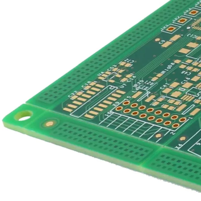
PCB prototyping is the process of producing physical circuit board samples from a preliminary design and evaluating their electrical performance, assembly quality, and suitability for manufacturing. A prototype may be fabricated and assembled in an in-house facility or by a specialized PCB manufacturing partner, depending on the project's requirements.
The purpose of PCB prototyping is to verify that the circuit works as intended before committing to full-scale production. Engineers can examine component placement, signal connections, board dimensions, and manufacturing details to uncover potential problems that may not be obvious during schematic or layout design.
By detecting and correcting issues at an early stage, companies can limit unnecessary material consumption, reduce production rework, and improve product reliability. A well-executed prototype also provides valuable feedback for refining the design and preparing it for repeatable manufacturing.
What are the Steps in PCB Prototyping?
PCB prototyping involves a sequence of coordinated activities, from defining project requirements to validating the assembled board. Designers, electrical engineers, assembly specialists, and PCB manufacturers may all contribute to the process. Each stage provides information needed to make the next stage more accurate and efficient.
The following steps outline a typical PCB prototyping workflow.
Requirements Planning. Begin by establishing the circuit's intended functions, operating environment, performance targets, size limitations, budget, and project schedule. These requirements guide decisions about component selection, PCB materials, layer count, and manufacturing methods. Identifying technical constraints early also helps reduce unnecessary design changes later.
Generation of PCB Schematics. Create the circuit schematic using electronic design automation (EDA) software such as Altium Designer or Autodesk EAGLE. The schematic defines the electrical relationships between components, including power connections, signal paths, and grounding. Engineers should verify component values, pin assignments, and connectivity before moving to physical layout design.
BOM Creation. Prepare a Bill of Materials (BOM) listing the components required for the prototype, including part numbers, specifications, quantities, and supplier information. Reviewing component availability and identifying suitable alternatives can help avoid procurement delays. The BOM also provides a useful reference for assembly planning and cost estimation.
Generation of PCB Layout. Translate the schematic into a physical board layout by arranging components and routing conductive traces. The design should account for board dimensions, component clearances, electrical requirements, thermal management, and assembly access. A carefully planned layout can improve signal integrity, simplify manufacturing, and make the final board easier to assemble and inspect.
Design Rule Check. Run a Design Rule Check (DRC) to identify layout issues that may prevent successful fabrication. Typical checks include minimum trace width, spacing between copper features, drill dimensions, annular rings, and board-edge clearances. Electrical Rule Check (ERC) can also be used during schematic development to identify potential connectivity or electrical-design problems. Both checks help resolve errors before manufacturing files are released.
Gerber File Generation. Export the PCB design data required by the selected manufacturer. Gerber files are widely used to communicate copper layers, solder mask, silkscreen, and other board information. Depending on the design and manufacturer's workflow, additional files may include NC drill data, board outlines, fabrication notes, and assembly drawings. Review the exported data before submission to ensure that it accurately represents the intended design.
PCB Fabrication. Submit the approved manufacturing files to a PCB fabrication facility, where the physical board is produced according to the specified materials, dimensions, and layer structure. Multilayer PCB fabrication involves several interconnected processes, which may include the following:
Lamination. The inner copper layers are patterned and prepared before the multilayer stack is bonded using heat and pressure. Prepreg and core materials help form a stable structure with the required electrical insulation between layers.
Drilling. Holes are drilled to accommodate component leads and electrical interconnections. Depending on the design, plated through-holes and vias connect selected copper layers. Drill sizes and positions must match the manufacturing data and the board's design requirements.
Etching and Solder Masking. Unwanted copper is removed to create the required circuit patterns. A solder mask is then applied over designated areas to protect the copper and reduce the risk of accidental solder bridging during assembly.
Surface Finish. An appropriate surface finish is applied to exposed copper pads to protect them from oxidation and support reliable soldering. The finish is selected according to component requirements, assembly processes, shelf-life expectations, and budget.
Silk Screening. Component references, polarity indicators, logos, and other identification markings are printed or applied to the board's silkscreen layer. Clear markings help assembly technicians position components correctly and simplify later inspection and maintenance.
Bare PCB Testing. Before components are installed, the fabricated board is checked for manufacturing defects. Electrical testing may identify unintended shorts, open circuits, or other connectivity problems. Dimensional and visual inspections can also be performed to verify that the board meets the specified requirements.
PCB Assembly. After fabrication and initial inspection, electronic components are mounted onto the prototype board. The assembly method depends on the component package types, board design, and production requirements. For a typical surface-mount assembly process, the main stages include:
Solder Paste Printing. Solder paste is deposited onto designated surface-mount pads through a stencil. Accurate paste volume and alignment help establish reliable solder joints during reflow.
Component Mounting. Components are positioned on the PCB according to the assembly data. Automated pick-and-place equipment is commonly used for surface-mount devices, while through-hole components may require a separate insertion and soldering process.
Reflow. The assembled board passes through a controlled heating profile that melts the solder paste and forms electrical and mechanical connections. The temperature profile must suit the solder alloy, components, and PCB materials.
Visual Inspection. The assembled prototype is inspected for issues such as misaligned components, solder bridges, insufficient solder, and damaged parts. X-ray inspection may be appropriate for hidden solder joints, including those beneath certain ball-grid-array packages. Inspection methods are selected according to the assembly design and quality requirements.
PCBA Testing. The completed printed circuit board assembly (PCBA) is evaluated against the project's functional and electrical requirements. Depending on the product, testing may include power-on checks, voltage measurements, signal verification, continuity testing, programming, and functional testing. Engineers investigate any failures, adjust hardware or firmware where necessary, and confirm that the revised assembly operates as intended.
Design Iterations. Prototype testing may reveal issues that require changes to the schematic, component selection, PCB layout, or assembly process. Engineers document the findings, implement appropriate revisions, and build or rework the prototype for another round of evaluation. This cycle continues until the design meets the defined acceptance criteria and is sufficiently mature for the next development stage.

What are the Benefits of PCB Prototyping?
Although prototype development requires additional time, materials, and engineering effort, it can help prevent more expensive problems during later manufacturing stages. The main benefits of PCB prototyping include improved manufacturability, stronger quality control, more efficient product development, and lower overall project risk.
Higher Yield. A PCB prototype allows engineers to identify design and assembly issues before large quantities of boards are produced. Potential problems involving trace spacing, component placement, thermal performance, and solderability can be corrected during development. When these issues are resolved early, the production design is more likely to pass manufacturing and assembly processes with fewer defects, helping improve overall yield.
Better Quality. Prototyping provides an opportunity to compare actual board performance with the original technical specifications. Engineers can evaluate electrical behavior, inspect solder joints, and investigate failures under relevant operating conditions. Feedback from these assessments helps refine the layout, materials, component choices, and assembly procedures, contributing to more consistent product quality.
Early Time-to-Market. Testing a design before mass production can shorten the overall development cycle by revealing problems while changes are still manageable. Early prototype feedback helps engineering teams prioritize corrections, coordinate with manufacturing partners, and prepare more complete production documentation. Although prototyping adds a development stage, it can reduce delays caused by major redesigns or manufacturing failures later.
Cost Saving. Producing a small number of prototype boards generally involves less financial exposure than discovering the same defect across a large production batch. PCB prototyping helps reduce wasted components, repeated fabrication runs, assembly rework, and potential product returns. It also allows teams to compare design alternatives and manufacturing options before committing to higher-volume orders.
Conclusion
PCB prototyping is an important step in turning an electronic design into a reliable, manufacturable product. By combining design verification, PCB fabrication, component assembly, and performance testing, businesses can identify potential issues before they become expensive production problems. A structured prototyping process supports better product quality, more predictable manufacturing, and more informed engineering decisions.